Abstract
Bio-applications of nanopillars are discussed, with a focus on the advantages nanopillared surfaces compared to flat surfaces and the properties of nanopillars behind each application are explained.
Introduction
In recent years, the potential applications of nanopillars have attracted significant attention. Nanopillar surfaces possess fascinating qualities that render them more valuable than conventional flat surfaces in bio-applications, such as medical treatments, neuronal pinning, biosensors, tissue engineering, DNA analysis, and antibacterial materials. The introduction of nanopillars has three effects on the biological processes on surfaces: increasing surface area, enhancing cell adhesion and growth, and ability to penetrate cells.
Nanopillars can be fabricated from two approaches: top-down and bottom-up. The top-down fabrication of nanopillars can be achieved by the traditional lithography, reactive ion etching (RIE), electron beam lithography (EBL), focused ion beam lithography (FIBL) etc. RIE is a highly anisotropic etching process. It can be used to fabricate nanopillars on substrates with high aspect ratios [1]. EBL and FIBL can achieve the fabrication accuracy of the level of sub 100nm.
Low cost top-down methods include nanosphere and nanoparticle lithography. In these methods, masks can be produced by assembling nanospheres or nanoparticles into close-packed arrays onto wafers by spin coating or the Langmuir-Blodgett method [2,3]. The spacing and diameter can be controlled by the size of the nanoparticles or nanospheres. Other lower cost techniques include diblock copolymer lithography, [2] anodized aluminum oxide (AAO) lithography, [4,5] colloid lithography, laser interference lithography etc. for specific fabrication application purposes [6,7].
The bottom-up approaches include chemical vapor deposition (CVD), [8] vapor-liquid-solid (VLS) growth, pulsed laser deposition, [9,10] template-assisted techniques, etc. [11-14]. Recently, small-molecule-based organic crystalline nanopillars are prepared by using self-assembled approaches [15,16]. We have also developed a surface-assisted self-assembly approach to harvest single-crystalline organic nanopillar semiconductors from a solution [17-19]. Fabrication of vertically nanopillars is simply done by using the self-assembled method, the materials of which range from, organic, such as an H-bonding system for self-assembly by triple hydrogen bonds from cyanuric acid (CA) and melamine derivatives. The nanopillars prepared by this method can be made in large quantities at a low cost due to the facile self-assembling method. This makes the method a viable option for preparing nanopillar-based devices or coatings. Other techniques include atomic force microscope (AFM) [20] UV assisted soft nanoimprint lithography [20] self-assembly combined with metal-assisted etching [21] template-assisted techniques [22] etc.
The materials for these nanopillars include silicon, metals, metal oxide [23,24]. ceramics, organic, and polymers [25]. It is noteworthy that the word ‘nanopillar’ is used in the paper; however, our interests also include pillars at submicro- or even micro- scales.
Increasing surface area
The unique capabilities of nanopillars are largely attributed to their structures and morphologies. The presence of many vertically aligned nanopillars on a lateral surface significantly increases the surface area without changing the overall dimensions of the original substrate [26]. The surface area of a nanopillared surface (S) can be calculated from the following equation:
 (1)
(1)
where S0 denotes the area of the original flat surface. The increase in surface area from the nanopillars is represented by the addition of n(2 rl), where r denotes the radius of each nanopillar, l is the height of the nanopillars, and n is the number of nanopillars on the flat surface. The increased surface area has various bioapplications, such as biosensing; if more receptors—such as antibodies, enzymes, or oligonucleotides—can be immobilized on a surface, a sensor based on this surface can interact with more target analytes, and thus demonstrate higher sensitivity. Likewise, in electrochemical biosensors, the greater active surface area of nanopillar electrodes increases the current output of the device, which also leads to higher sensitivity.
Enhancing cell adhesion and growth
Nanopillars also possess a unique geometry that strengthens their interaction with cells. The placement of nanopillars in an ordered array encourages cells to position themselves in between pillars while wrapping the ends of their membranes around the pillars for increased support. This essentially creates a “pinning” effect by which the cell fastens itself to the nanopillars [27]. Focal adhesions are created between the cells and the pillars, which strengthen cell adhesion. Moreover, nanopillars can also trigger an increase in the density of adsorbed globular proteins such as collagen (a key extracellular protein), which further enhances cell adhesion [28]. This property is helpful for applications in tissue engineering, such as medical implants. To achieve seamless integration between medical implants and the body, nanopillar surfaces can be applied due to the strong interaction between nanopillar topographies and adherent cells. The nanopillar-cell interaction is also useful for neurons, which must be pinned due to their constant firing and relaxation.
As aforementioned, the topography of nanopillar surfaces can cause changes in the placement and conformations of adherent cells. This effect has also been shown to induce adherent cells to upregulate the expression of proteins and other metabolites that support cell growth and development [29]. The mechanism of biomolecule upregulation by nanopillars has not been clearly reported. However, noted examples of upregulated biomolecules include differentiation transcription factors and vital amino acids. As a result, many studies hypothesized that nanopillars will improve cell growth and proliferation. The use of topographical cues to develop cells also contributes to applications in tissue engineering.
Ability to penetrate cells – with positive or negative effects on cells
The shape of nanopillars also contributes to their remarkable abilities. Due to their tapered pointed ends, some nanopillars have demonstrated the ability to penetrate cells. For instance, nanopillars can safely penetrate living cells to deliver important biomolecules that are linked to the ends of the nanopillars [30]. This method can be used in delivering drugs directly into cells, eliminating the need to administer medications orally or inject them into the blood stream. This is particularly useful for medications that readily decompose inside the body before even reaching their target. The pointed ends can also function as a defense mechanism to kill bacteria by rupturing the membranes of adherent bacterial cells. This quality is also useful in antibacterial applications, such as manufacturing medical implants [31,32]. The current method of using chemically treated implants can lead to more serious issues like resistant bacterial strains. Nanopillars can serve as an improved defense mechanism against bacterial infections that may develop after medical implants are inserted in the body.
In this summary, various bio-applications of nanopillars are discussed, focusing on the advantages of the three effects discussed above. The properties of nanopillars behind each application are explained.
Medical treatments
It is important to develop localized drug delivery to improve the state of medical treatment. Administering drugs locally not only mitigates side effects and drug toxicity but also maximizes drug performance. Nanopillar array substrates (Figure 1) were recently created to enhance the efficacy of drug delivery systems [33]. The efficacy of the delivery process is directly linked to endocytosis. To this end, it was hypothesized that nanopillars could topographically enhance cellular endocytosis. To test this, human mesenchyme stem cells (MSC) were cultured on nanopillars and subsequently incubated in a dextran-containing medium. The study revealed that MSCs cultured on 200-nm tall nanopillars initially internalized more fluorescently labelled dextran molecules before eventually equalizing with the other surfaces (Figure 2). The increased endocytosis occurs because, unlike flat surfaces, the nanopillar topography influences the cellular expression of endocytosis-related proteins such as caveolin-1 and clathrin. Caveolae- and clathrin-mediated endocytosis are two major pathways used to deliver drugs to cells. Therefore, nanopillars may offer the potential to enhance drug transport for at least the short term. The advantage of nanopillar-based drug delivery is that these systems can deliver greater drug doses than conventional flat surfaces immediately after introducing a drug. The results of this study offer promising hope for future development of improved delivery vehicles for drugs like doxorubicin, an anti-cancer medication used by thousands of patients.
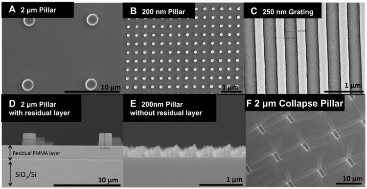
Figure 1. Scanning electron microscopy of poly(methly methacrylate) (PMMA) nano- and micro-structures used in this study showing (A) 2 mm diameter pillar with 2 mm height (top view), (B) 200 nm diameter pillar with 400 nm height(top view), (C) 250 nm grating with 250 nm height (top view), (D) 2 mm PMMA pillars with residual layer (cross sectional view), (E) 200 nm Rhodamine-PS pillar without residual layer (cross sectional view) and (F) 2 mm Rhodamine-polystyrene collapse pillar (Top view). Reprinted with permission from Teo, et al., Biomaterials 32, 9866 [34] ©2011 Elsevier B.V.
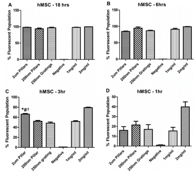
Figure 2. Flow cytometry analysis of FITC-dextran internalization in hMSC cultured on 2 mm pillars, 200 nm pillars and PMMA control (1 mg/ml). PMMA control (2 mg/ml) represents the positive control for the experiment. The percentage of fluorescent hMSC population was analyzed at (A) 18 h, (B) 6 h, (C) 3 h and (D) 2 h of incubation time. hMSCs that were cultured on 2 mm pillars after 3 h of incubation time showed a significantly increased dextran internalization compared to 200 nm pillars, 250 nm gratings and 1 mg/ml PMMA control. Reprinted with permission from Teo, et al., Biomaterials 32, 9866 [34]. ©2011 Elsevier B.V.
Metastasis occurs when circulating tumor cells (CTCs) break away from the primary tumor and travel to other tissues. Monitoring the level of CTCs provides critical information regarding the status of a growing cancer. Needless to say, it is vital to develop sound techniques to control a growing tumor. Commercially available methods to capture CTCs is ineffective because CTCs exist in very small numbers in the blood stream. To detect and capture these migratory cells, Wang et al. [34] developed silicon nanopillars through lithography and chemical etching. The structures were subsequently coated with anti-EpCAM (epithelial cell adhesion molecule antibody), a cancer cell capturing agent. Compared to flat surfaces, the nanopillars demonstrated a superior ability to capture CTCs (>95%), due to enhanced local interactions between the anti-EpCAM coated silicon pillars and cancer cell surface components. Silicon wafers with anti-EpCAM grafted nanopillars were fabricated through chemical etching. For nanopillars with a diameter of 100-200 nm, a CTC isolation efficiency of 95% was reported. The greater surface area of the nanopillars increased the odds of binding between the immobilized EpCAM antibodies and cancer cell surface receptors. These results were further supported by a more recent study from the same group [1]. As nanopillar-based systems are clearly more effective than flat surfaces in capturing CTCs, future commercialization of these devices will assist in detecting and treating metastasis in cancer patients.
Neuronal growth and pinning
Nanopillar technology has been used to assist in the growth of neurons. This technology can be useful for treating neurodegenerative diseases. Current methods of using biochemical factors to induce differentiation on smooth surfaces is problematic because some stem cells may be left undifferentiated. They can even become carcinogenic. It is also difficult to regulate the optimum environment needed for the biochemical factors to function. Migliorini et al. [1] fabricated silicon nanopillars to trigger embryonic stem cell differentiation into neurons. By taking advantage of the cell-substrate interaction of nanopillars, they hypothesized that nanopillar topography would augment the differentiation of embryonic stem cells, which is helpful in regenerative growth treatments. After 6 hours of incubation, the nanopillars (33 +/- 2.7%) exhibited more than twice the neuronal yield on flat substrates (13 +/- 0.8%). Increased cell differentiation was observed because (i) nanopillars are more compatible with the cell extracellular matrix and (ii) the nanopillars can easily adapt to accommodate the structure of the neurons by altering the expression of integrins and focal adhesion proteins. The cell-substrate interaction between stem cells and nanopillars is more conducive to differentiation. Therefore, this technology can be applied in treating degenerative nerve diseases, where neuronal cell differentiation is vital.
In addition to their ability to support neuronal growth, nanopillars can also be used in neuronal pinning. By nature, neurons are frequently triggered and relaxed, so they are susceptible to excessive migration. This means there is a greater need to “pin” them down during study. It was hypothesized that culturing neurons on nanopillars would secure the cells in place. To this end, Xie et al. [35-37] developed nanopillars that significantly diminish cell migration without impairing the condition of the neurons. Platinum was coated on the nanopillar due to its biocompatibility, as well as its ability to directly measure the electrical signals of neurons. The dimensions of the nanopillars were 150 nm in diameter and 1 μm in height. Following a 5-day observation period, they found that unrestricted neurons moved 57.8 μm on average, while nanopillar-pinned neurons demonstrated an average migration of 3.9 μm (Figure 3). Nanopillars act as focal adhesion points for the neurons, eliminating the need for special cell-loading processes. They also observed that the neuronal cell membrane tends to wrap around the nanopillars (Figure 4); this essentially “pins” the neuron to the pillars, enabling researchers to follow the development a single neuron over an extended period of time.
Figure 3. Statistics of cell migration over 5 days. (a) Typical movement traces of four nanopillar-pinned and four free-migrating neurons. Bottom right plot shows zoom-in of the nanopillar-pinned cell movements. While the free-migrating neurons explore ∼60 µm distances, the nanopillar-pinned cells move no more than 5 µm. (b) Analysis of neuron movements over 42 free-moving and 21 nanopillar-pinned neurons show that nanopillars effectively stopped the migration of neurons. Reprinted with permission from C. Xie et al., Nano Lett 10, 4020 [38]. ©2010 ACS
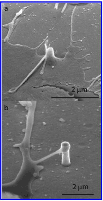
Figure 4. SEM of cells cultured on Si and SiO2 nanopillar substrates. (a) An SEM image shows a SiO2 pillar engulfed by the cell membrane. (b) An SEM image shows a protruding of a neuron reaching a Si nanopillar. Reprinted with permission from C. Xie et al., Nano Lett 10, 4020 [38]. ©2010 ACS.
In another study, Kwait et al. [38] used silicon nanopillars to cultivate mature, robust neuronal networks in predetermined patterns. The pillars were spaced 4 μm apart using e-beam lithography. The final nanopillars were measured 70-100 nm in diameter and 1 μm in height. After chemically modifying the nanopillars with flurosilane and polylsine, cortical neuronal rat cells were grown on the pillared surface. The neuronal network—consisting of cell bodies, axons, and dendrites that were positioned directly on the pillars—remained intact for more than 14 days. This novel procedure may enable complex neural networks to be constructed for in vitro studies of individual neurons and their interactions. It is a vast improvement over the current techniques for directed neuronal growth, which are sometimes unable to hold neurons in place.
Signal enhancement in biosensors
One of the most important applications of nanopillars is for use in bio-sensing. A biosensor uses receptors to recognize a target analyte and the recognition could result in a signal that can be measured. The unique properties of nanopillars can improve the functionality of biosensors in many ways, such as lowering the minimum detection limit or enhancing the signals produced by the sensor because of the enhanced active surface area of nanopillars, which increases the signal-to-noise ratio of the sensor, leading to enhanced sensitivity. In some cases, they also improves accuracy of biosensors, which provides key information about metabolic and physiological processes in the body.
Anandan et al. [39] fabricated vertical nanopillars for electrochemical biosensing. Based on their results, they concluded the major reason that nanostructured electrodes can drastically improve the viability of electrochemical biosensors is the much greater active surface area of the electrode, which resulted in a significantly greater amperometric response than the flat electrodes. This makes the nanostructured biosensor more sensitive. Furthermore, they also found that the nanopillars had sufficient mechanical strength to withstand capillary forces in the body’s aqueous environment, which is required for the biosensor to function effectively.
Chen et al. [40] fabricated nanopillar arrays for DNA detection by using very-large-scale integration method (VLSI) and reactive ion etching (RIE). Oligonucleotides were crosslinked on the nanopillars to detect target single strand DNA (ssDNA). They reported that the resulting nanostructure could selectively locate and bind to target ssDNA while preserving its function and properties, and the 3D surface area enhances the immobilization capacity of oligonucleotides. As a result, when compared to flat surfaces, the nanopillar-based sensor increased target accessibility that resulted in higher selectivity and sensitivity. This nanopillar-based sensing scheme is also cheaper and less time-consuming than current labelling methods (i.e., fluorescence). Current labelling methods largely encounter steric hindrance, which limits their ability to identify ssDNA. The cost-effective nanopillar-based detection scheme is, therefore, more viable for future commercialization.
Saito et al. [41] used thermal nanoprint lithography to imprint nanopillars onto a Cyclo-olefin polymer (COP). Gold was also coated on the nanopillars, followed by grafting of antibodies against human immunoglobin. The biosensing ability of the nanostructured sensor was demonstrated by a test for Human immunoglobin protein. The Au-capped nanopillar array exhibited a minimum detection limit of 6.7 × 10⁻³ nM, which is much lower than the 1 nM detection limit from flat sensors. The increased sensitivity is attributed to a greater surface area as well as localized surface plasmon resonance.
A recent reported surface acoustic wave (SAW) sensor [42] based on Cobalt phthalocyanine (CoPc) nanopillars for detection of dopamine, a neurotransmitter, also showed a better sensitivity. In comparison to a flat sensor, the CoPc nanopillar sensor possessed a greater maximum surface peak height, which increased its sensitivity. Furthermore, current electrochemical methods to detect dopamine are particularly problematic because the neurotransmitter usually coexists with high levels of ascorbic acid, which interferes with the ability of the biosensor to recognize only dopamine. The nanopillar device, however, was selective towards dopamine due to stronger interactions between dopamine and CoPc nanopillars. The geometry of dopamine favored its interaction with CoPc nanopillars because the occupied π orbital on the nitrogen atom of dopamine overlaps perfectly with CoPc. The ability to detect traces of dopamine makes the nanopillar-based biosensor a commercially favorable idea.
Nanopillars have also been used to enhance the assay signals. Kandziolka et al. [43] reported that nanopillars strengthened the signal intensity of the fluorescent assay because of a larger surface area. Their study showed that a substrate sample with 1 labelled BSA per 1000 unlabeled BSA still produced an acceptable Signal-to-Noise ratio (SNR) of 5.5, indicating that nanopillars may provide a minimum detection limit as low as one molecule.
Due to a diameter (150 nm diameter; 700 nm in height) that is much smaller than the wavelength of visible light, Xie et al. [44] fabricated vertically aligned nanopillars (Figure 5) that limited the transmission of light and created a vertical evanescence wave effect and led to a highly localized luminescence. Only molecules in the immediate surroundings of the nanopillars were illuminated. These unique properties were not seen on flat surfaces. As the radial distance from the nanopillar increased, the light intensity decreased exponentially, supporting the idea that the nanopillar emits a highly localized and intense light (Figure 6). This property of the vertical nanopillar is useful for detecting only a small number of molecules in a complex cellular environment. The ability of nanopillars to enhance the precision and sensitivity of fluorescence detection is advantages in biosensing. It’s likely that this technology can be applied in biological or medical research, where fluorescence microscopy is of key significance.
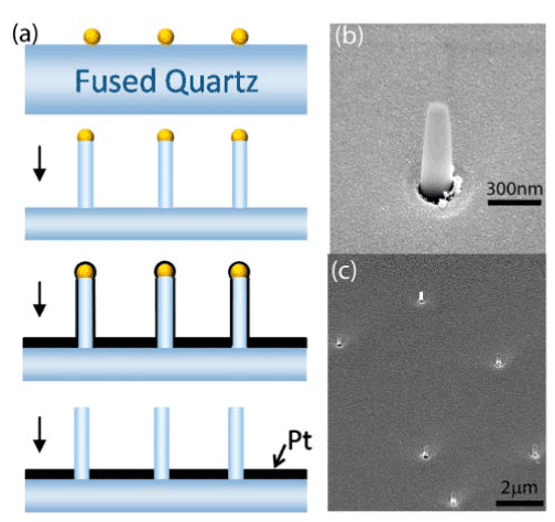
Figure 5. Fabrication of the SiO nanopillars. (A) Schematic illustration of the fabrication process with gold nanoparticles as etching masks. (B) Typical SEM image of a nanopillar with viewing angle at 52°. (C) SEM image of randomly dispersed nanopillars with viewing angle at 52°. The average distance between nanopillars is about 3–5 µm. Reprinted with permission from C. Xie et al., PNAS 108, 3894-3899 [45] ©2011 PNAS
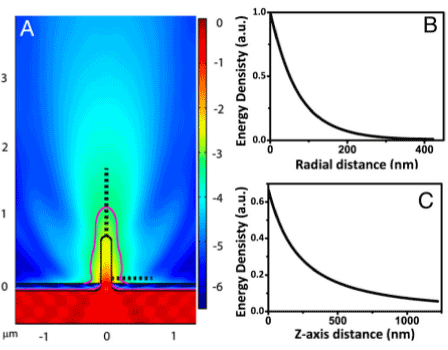
Figure 6. Illumination profile surrounding a nanopillar. (A) Finite-element analysis of the intensity distribution for a nanopillar of 150 nm in diameter and 700 nm long. Purple line indicates the contour of 1∕e2 intensity (the intensity at the nanopillar surface 100 nm away from the platinum substrate is designated to be 1). (B) Plot of the light intensity as a function of radial distance along the horizontal dash line in A.
The greater surface area of nanopillars have also been shown to enhance the functionality of DNA sensing devices. In a study conducted by Murthy et al., [45] silicon dioxide nanopillars (Figure 7) demonstrated the ability to improve DNA microarrays because of a greater capacity of oligonucleotide probes to be placed on the nanopillars. As the concentration of oligonucleotide probes increased, the nanopillars demonstrated a higher SNR in comparison to the other substrates (Figure 8). This suggests that nanopillars are more effective than planar substrates for detection at lower concentration due to an increased probe capacity and a greater SNR.
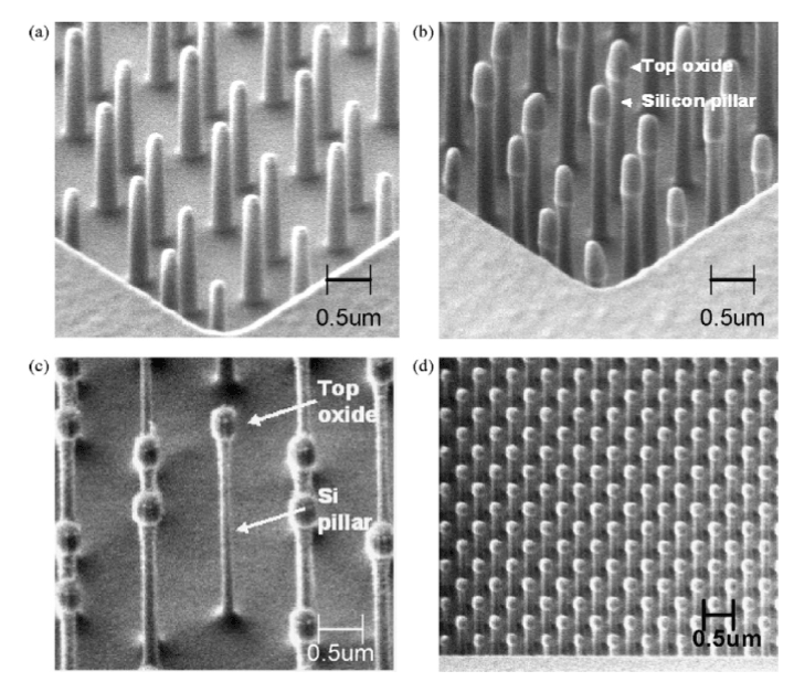
Figure 7. SEM images of the nanopillars. (a) Single-substrate nanopillars consisting SiO2 (b) Dual substrate nanopillars consisting SiO2 layer atop the Si pillar. (c) Very high-aspect ratio dual-substrate nanopillars. (d) Dense array of ordered dual-substrate. Reprinted with permission from Murthy et al., Biosensors Bioelectronics 24, 723–728 [35] ©2008 Elsevier B.V.
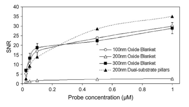
Figure 8. Effect of immobilized probe concentrations on SNRs for 100, 200, and 300 nm thin oxide blanket substrates and 200 nm dual-substrate nanopillars. Reprinted with permission from Murthy et al., Biosensors Bioelectronics 24, 723–728 [35] ©2008 Elsevier B.V.
Kim et al. [46] also demonstrated enhanced sensor performance for DNA detection. They observed that as the height of pillars in the nanoarray increased, the signal intensity also improved due to the larger active surface area. The nanoarray possessed a surface area 4 times greater than that of the planar substrate, which caused a three-fold increase in signal intensity of the DNA sensor. The results imply that nanopillars have a marked ability to strengthen the efficacy of biosensors.
DNA separation
The separation of DNA is an important process in genetic analysis. It is widely used in many applications such as medical diagnosis or crime scene investigations. Customary gel electrophoresis, in which smaller fragments also migrate faster due to lighter size, is unable to separate large DNA fragments. The process requires ample time to separate DNA. Using nanostructured devices for DNA separation solves these issues. Due to their highly ordered nature, nanopillar arrays were hypothesized to function as a DNA sieving tool. Larger molecules can now be separated in a matter of seconds.
Kaji et al. [47] fabricated nanopillars on a quartz plate through e-beam lithography (Figure 9). The dimensions of the nanopillars were 100-500 nm in diameter and 500-5000 nm in height. An electric field was applied to initiate the migration of DNA through the nanopillar array. The molecules migrated at different rates according to their size – smaller DNA fragments travelled farther than larger fragments, because larger DNA fragments frequently collided with the nanopillars and changed conformations by uncoiling (Figure 10). Smaller fragments did not collide into any pillars, so they remained in the same coiled conformation. This explains the ability to separate the fragments efficiently through the nanopillar array. The nanopillar-based DNA separation is more effective because nanopillars can separate long DNA fragments (~40 kbp) in just a few seconds.
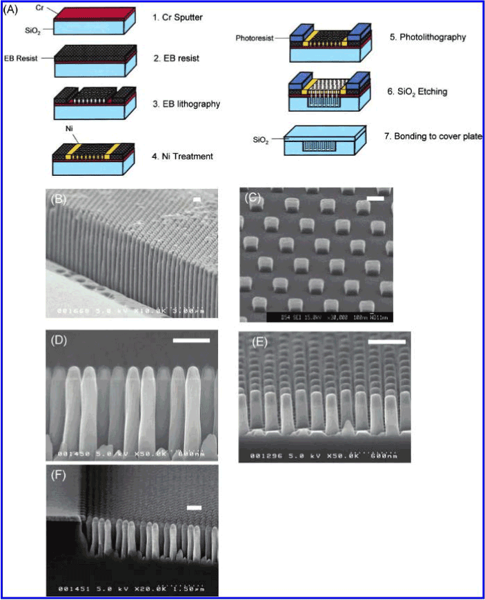
Figure 9. (A) Schematic description of nanofabrication processes. (B-E) Nanopillar structures fabricated on a quartz glass plate before sealing by a cover plate. The nanopillars dimensions were 200 nm wide and 4000 nm tall (aspect ratio, 20), 500 nm wide and 500 nm tall (aspect ratio, 1), 200 nm wide and 1200 nm tall (aspect ratio, 6), and 200 nm wide and 600 nm tall (aspect ratio, 3) in (B-E), respectively. (F) Nanopillar channel fabricated with Cr mask for SiO2 dry etching. Damaged Cr mask during NLD caused a nonuniform etching and results in rugged sidewall nanopillars. The scale bars are all 500 nm. Reprinted with permission from Kaji et al., Anal. Chem. 76, 15-22 [48] ©2004 ACS.
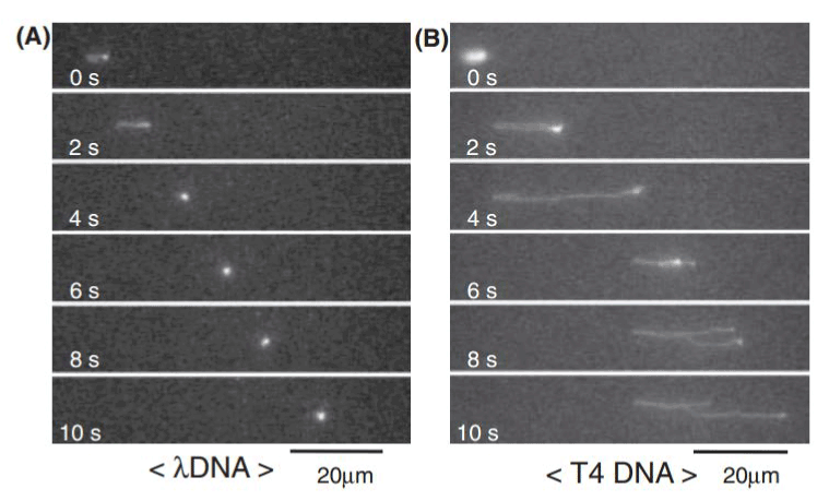
Figure 10. An imaging of a single DNA molecule migrating in the nanopillar device. Reprinted with permission from Kaji et al., Anal. Chem. 76, 15-22 [48] ©2004 ACS.
A more recent study [48] also demonstrated that nanopillars allowed the rapid separation of large DNA fragments for applications in DNA studies involving lengthy DNA fragments. The study concluded that DNA separation with nanopillars is 100-fold faster than gel electrophoresis. A study by Yasui et al. [49] further supported this conclusion using nanopillars.
Wang et al. [50] incorporated nanopillars into a microfluidic channel. Their study showed that lambda-DNA molecules are partially stretched in the microfluidic channel due to the “retractive force” of the fluid and the hydrophobic force from the surface acting upon the molecule. Other than separation, stretching out the DNA also enables researchers to closely examine the molecule. In a similar study by Kuo et al., [51] the lambda DNA molecules were measured to stretch up to 16 nm (the full contour length of lambda DNA is 16 nm).
Tissue engineering
The three important factors in the development of tissue engineering technology include cell adhesion, cell growth, and cell proliferation. Nanopillars, which have been shown to improve these three factors, are highly regarded for applications in medical implants and tissue regeneration schemes.
In the past decade, a multitude of studies have successfully demonstrated the cell adhesion ability of nanopillars. Hu et al. [52] showed that after dermal cells were cultured on the nanopillars, no cell mobility on the surface was observed because the cells formed robust adhesion complexes with the nanopillars. Brammer et al. [53] achieved similar results from mesenchyme stem cells (MSCs) that were grown more effectively on nanopillars. Compared to flat topography, the nanopillars exhibited a significantly greater cell adhesion after just 2 hours of incubation. In another study, Kim et al. [54] showed that the polyethylene glycol (PEG) nanopillar arrays (132 cells/mm2) had a cell adhesion of more than three times greater than that of the planar PEG substrate (39 cells/mm2). A study by McNamara, et al. [55] achieved similar results to those of Hu, Brammer, and Kim. After culturing MSCs, their study showed that MSCs formed larger focal adhesions on 15 nm nanopillars, providing more evidence that nanopillars can promote cell adhesion.
The increased cell adhesion were explained by greater hydrophobicity and nano feature size of nanopillars. Hydrophobic surfaces can increase the amount of adsorbed collagen, an important extracellular matrix protein that can strengthen cell adhesion. Meanwhile, decreasing the surface feature size to the nanoscale increases the density of adsorbed globular proteins, which also enhances cell adhesion.
In addition to cell adhesion, nanopillars have also exhibited the ability to influence the growth and development of new cells. Padeste et al. [56] found that, after culturing mice neural stem cells on nanopillars, the cells can sense their location on the nanopillars and respond accordingly by positioning themselves in between pillars, which may be a mechanism to maximize the cell-surface contact area. The fact that the cell growth is influenced by the conformations of nanopillar arrays was further explored in later studies to ultimately discover that nanopillars are able to promote cell growth and proliferation. For example, McNamara, et al. [57] found that Runx2, a transcription factor regulating differentiation, was more expressed in cells cultured on 15 nm pillars (Figure 11 and 12). The 15 nm nanopillars are also responsible for the upregulation of key amino acids that are vital to metabolic processes that support cell development. These mechanisms, which were less apparent in cells cultured on flat substrates, explain the enhancement of cell #differentiation by nanopillars.
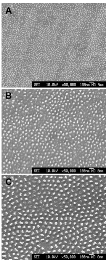
Figure 11. SEM images of the test surfaces. (A) 15 nm high Ti oxide nanopillars, (B) 55 nm high nanopillars and (C) 90 nm high nanopillars. Reprinted with permission from McNamara et al., Biomaterials 32, 7403-7410 [48] ©2011 Elsevier B.V.
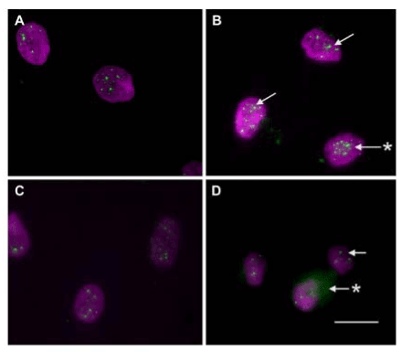
Figure 12. Phospho (pS469)-Runx2 was examined in cells on planar (A), 15 nm high (B), 55 nm high (C) and 90 nm high (D) titania nanopillar-like structures. Cell spreading was greater on the planar and 15 nm structures, and the highest clustering (arrows in B) and abundance (* in B) of nuclear phospho-Runx2 was detected in cells on the 15 nm high pillars, with the least phospho-Runx2 on the 90 nm surface (arrow). Some cells had greater cytoplasmic staining on the 90 nm surface (* in D), likely to represent the transcription factor that had been shuttled out of the nucleus.
In another study, Loya et al. [58] cultured endothelial aortic cells on a nanopillar array (Figure 13) on a metallic stent. Current metal stent technology is problematic due to the risk of late-stent thrombosis, which occurs due to lack of endothelial cell coverage on the bare metal stent. Loya’s study showed that the nanopillar surface significantly enhanced endothelial cell growth because the presence of nanopillars strengthened the endothelial cells through strong transmembrane tight junctions. The number of adherent endothelial cells on nanosurfaces was consistently greater than that on plain surfaces (Figure 14). With increased endothelial cell growth, the nanopillar stent is more seamlessly integrated with the blood vessel, thereby reducing the risk of thrombosis. Due to their unique properties, nanopillars are more supportive of cell growth, and therefore serve as an effective method of developing safer metallic stents in the future.
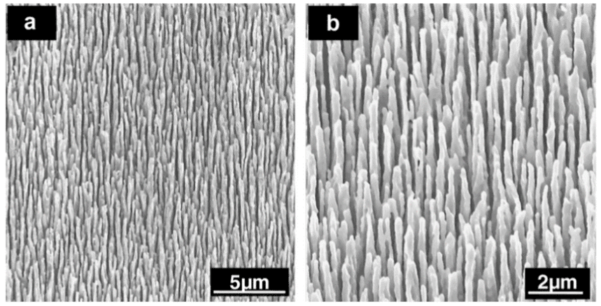
Figure 13. SEM micrograph depicting the high aspect ratio pillar nanostructure. This modified surface morphology on flattened MP35N stent alloy bare metal wire is the result of RF plasma processing. The image on the left (a) is a low magnification picture, while the image on the right (b) is at higher magnification. Reprinted with permission from Loya et al., Acta Biomaterialia 6, 4589-4595 (2010). ©2010 Elsevier B.V.
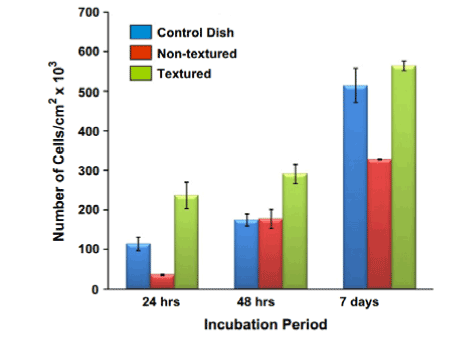
Figure 14. Cell number (normalized by sample size area) vs. incubation time. The bar graph shows the average +/- standard deviation. The textured surface has the highest adhesion after 24 and 48 h incubation. Reprinted with permission from Loya et al., Acta Biomaterialia 6, 4589-4595 (2010). ©2010 Elsevier B.V.
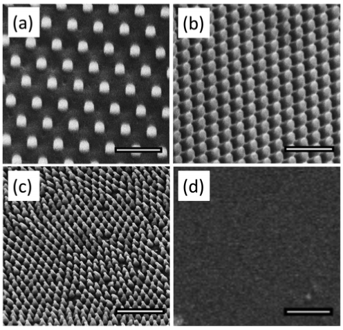
Figure 15. Micrographs of PMMA surfaces taken at 5 kV with the FEI Quanta 3D SEM. We used commercial molds to generate nanopillars in two different sizes, referenced here by periodicity: P600 shown in (a) and P300 shown in (b). We also used a two-step lithography process to replicate the nanostructures on the surface of the cicada wing in PMMA, referenced as P200, shown in (c). Images (a)–(c) were taken at a 30 tilt while the flat control (d) was taken at 0 tilt. All scale bars ¼ 1 lm. Reprinted with permission from Dickson et al., Biointerphases 10, 1-8 (2015) ©2015 AIP.
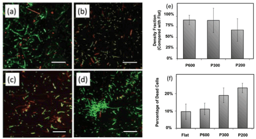
Figure 16. Live-dead assay micrographs are representative micrographs on (a) P600, (b) P300, (c) P200, and (d) the flat control. Live cells are tagged with green fluorescent SYTO9 while dead cells are tagged with red fluorescent propidium iodide. Scale bars ¼ 30 lm. (e) There is a decreased cell density on pillared surfaces compared to control flat surfaces, more so on smaller, more closely spaced pillars. Error bars represent the standard deviation of all samples. (f) The percent of cells on the surface that are dead is greater on pillars than on the flat.
Antibacterial
Recent studies have also demonstrated the remarkable ability of nanopillars to deactivate bacteria. Currently, many medical implants are susceptible to bacterial infection inside the body. Chemical treatments may cause unintended issues such as the development of drug-resistant bacterial strains.
The inspiration for this application comes from the Clanger cicada (Psaltoda claripenni), an insect whose wings possess nanopillars [59]. The wings serve as a natural defense mechanism against bacteria, so it was hypothesized that manmade nanopillars would exhibit similar antibacterial properties. To this end, a study by Dickson et al. [60] showed that after E.coli cells were cultured on the nanopillared surface (Figure 15), the nanopillars negatively impact the growth of the E.coli cells. Their study showed that nanopillar surfaces killed more bacterial cells than flat surfaces did (Figure 16). A closer analysis of the mechanism reveals that nanopillars actually penetrate the membranes of adherent bacterial and rupture the cells, leading to their demise. Flat surfaces cannot penetrate the bacteria, and thus lack of antibacterial activity. Another study [61] reported similar results using a polyethylene terephthalate (PET) nanopillar array fabricated by inductively coupled plasma (ICP). It was found that an interpillar spacing above 50 nm led to diminished bacterial cell adhesion. However, when the interpillar spacing was smaller than the diameter of the bacteria (<50 nm), the nanoarray actually supported bacterial adhesion due to the increased contact area between the cells and nanosurface. As the interpillar spacing approached the length of the bacterial cell diameter, the PET nanopillar array inhibited the growth of bacteria.
Figure 13. SEM micrograph depicting the high aspect ratio pillar nanostructure. This modified surface morphology on flattened MP35N stent alloy bare metal wire is the result of RF plasma processing. The image on the left (a) is a low magnification picture, while the image on the right (b) is at higher magnification. Reprinted with permission from Loya et al., Acta Biomaterialia 6, 4589-4595 (2010). ©2010 Elsevier B.V.
Conclusion
The vertically aligned nature of nanopillars offer significantly greater advantages than regular, planar surfaces. The unique and advantageous properties of nanopillars have already been effectively employed in bio-applications such as medical treatments, neuronal pinning, biosensing, tissue engineering, and antibacterial materials. The promising results seen in recent studies serve as a strong foundation for future applications of nanopillars.
References
- DeJarld M, Shin JC, Chern W, Chanda D, Balasundaram K, et al. (2011) Formation of high aspect ratio GaAs nanostructures with metal-assisted chemical etching. Nano Lett 11: 5259-5263. [Crossref]
- X Li, Tadisina ZR, Gupta S (2009) Preparation and properties of perpendicular CoPt magnetic nanodot arrays patterned by nanosphere lithography. J Vac Sci Technol A 27: 1062-1066.
- Marquestaut N, Martin A, Talaga D, Servant L, Ravaine S, et al. (2008) Raman enhancement of azobenzene monolayers on substrates prepared by Langmuir-Blodgett deposition and electron-beam lithography techniques. Langmuir 24: 11313-11321.
- Park HJ, Kang MG, Guo LJ (2009) Large area high density sub-20 nm SiO (2) nanostructures fabricated by block copolymer template for nanoimprint lithography. ACS Nano 3: 2601-2608. [Crossref]
- Kim DS, Lee HU, kim NH, Lee KH, Cho DW, et al. (2007) Fabrication of microchannel containing nanopillar arrays using micromachined AAO (anodic aluminum oxide) mold, Microelectronic engineering 84: 1532-1535.
- Skupinski M, Johansson A, Jarmar T, Razpet A, Hjort K, et al. (2008) Carbon nanopillar array deposition on SiO2 by ion irradiation through a porous alumina template. Vacuum 82: 359-362.
- Rafiq MA, Mizuta H, Uno H, Durrani ZAK (2007) Fabrication of vertical nanopillar devices, Microelectronic engineering 84: 1515-1518.
- Tanaka H, Shinkai M, Shibutani Y, Kogo Y (2009) Nonlinear large deflection of nanopillars fabricated by focused ion-beam induced chemical vapor deposition using double-cantilever testing. J Vacuum Sci Tech B 27: 2161-2165.
- MacManus-Driscoll JL, Zerrer P, Wang H, Yang H, Yoon H, et al. (2008) Strain control and spontaneous phase ordering in vertical nanocomposite heteroepitaxial thin lms. Nat Mater 7: 314–320.
- Zavaliche F, Zhao T, Zheng H, Straub F, Cruz MP, Yang PL, et al. (2007) Electrically assisted magnetic recording in multiferroic nanostructures. Nano Lett 7: 1586–1590.
- Skupinski M, Johansson A, Jarmar C, Razpet A, Hjort K, et al. (2008) Carbon nanopillar array deposition on SiO2 by ion irradiation through a porous alumina template. Vacuum 82: 359-362.
- Marquestaut N, Martin A, Talaga D, Servant L, Ravaine S, Reculusa S, et al. (2008) Raman enhancement of azobenzene monolayers on substrates prepared by Langmuir-Blodgett deposition and electron-beam lithography techniques” Langmuir 24: 11313-11321.
- Rafiq H, Mizuta S, Uno, Durrani ZAK (2007) Fabrication of vertical nanopillar devices. Microelectron Eng 84: 1515-1518.
- Park HJ, Kang MG, Guo LJ (2009) Large area high density sub-20 nm SiO (2) nanostructures fabricated by block copolymer template for nanoimprint lithography. ACS Nano 3: 2601-2608. [Crossref]
- Jiang L, Fu F2021 Copyright OAT. All rights reservtalline, size, and orientation controllable nanowires and ultralong microwires of organic semiconductor with strong photoswitching property. J Am Chem Soc 130: 3937–3941.
- Xiao K, Rondinone AJ, Puretzky AA, Ivanov IN, Retterer ST, et al. (2009) Growth, patterning, and one-dimensional electron-transport properties of self-assembled Ag-TCNQF4 organic nanowires. Chem Mater 2: 4275–4281.
- Ji HF, Xu X (2010) Hexagonal organic nanopillar array from the melamine-cyanuric acid complex. Langmuir 26: 4620-4622. [Crossref]
- Kojtari P, Carrol H.-F Ji (2010) Fabrication of Metal Organic Framework (MOF) Micro/Nanopillars – Towards Electronic and Optoelectronic Applications of MOFs. Chem Comm accepted.
- Wiesauer K, Springholz G (2000) Fabrication of semiconductor nanostructures by nanoindentation of photoresist layers using atomic force microscopy. J Appl Phys 88: 7289-7297.
- Shi J, Peroz C, Peyrade D, Salari J, Belotti M, et al. (2010) Tri-layer soft UV pmprine lithography and fabrication of high density pillars. Microelectronic Engineering 83: 1664-1668.
- Boarino L, Imbraguglio D, Eneico E, Leo ND, Celegato F, et al. (2011) Fabrication of ordered silicon nanopillars and nanowires by self-assembly and metal-assisted etching. Phys Status Solidi A 208: 1412-1416.
- Chen G, Soper SA, McCarley RL (2007) Free-standing, erect ultrahigh-aspect-ratio polymer nanopillar and nanotube ensembles. Langmuir 23: 11777-11781. [Crossref]
- MacManus-Driscoll JL, Zerrer P, Wang H, Yang H, Yoon J, et al. (2008) Strain control and spontaneous phase ordering in vertical nanocomposite heteroepitaxial thin ? lms. Nat. Mater 7: 314–320.
- Zavaliche F, Zhao T, Zheng H, Straub F, Cruz MP, et al. (2007) Electrically assisted magnetic recording in multiferroic nanostructures. Nano Lett 7: 1586-1590. [Crossref]
- Thonke K (2003) Polymer based nanopillars polymer-defined semiconductor nanostructures. Adv Solid State Phys 43: 155–170.
- Anandan V, Rao YL, Zhang G (2006) Nanopillar array structures for enhancing biosensing performance. Int J Nanomedicine 1: 73-79. [Crossref]
- Xie C, Hanson L, Xie W, Lin Z, Cui B, et al. (2010) Noninvasive neuron pinning with nanopillar arrays. Nano Lett 10: 4020-4024. [Crossref]
- Brammer KS, Choi C, Frandsen CJ, Oh S, Jin S (2011) Hydrophobic nanopillars initiate mesenchymal stem cell aggregation and osteo-differentiation. Acta Biomater 7: 683-690. [Crossref]
- Kim DH, Kim P, Song I, Cha JM, Lee SH, et al. (2006) Guided three-dimensional growth of functional cardiomyocytes on polyethylene glycol nanostructures. Langmuir 22: 5419-5426. [Crossref]
- Shalek AK, Robinson JT, Karp ES, Lee JS, Ahn DR, et al. (2010) Vertical silicon nanowires as a universal platform for delivering biomolecules into living cells. Proc Natl Acad Sci U S A 107: 1870-1875. [Crossref]
- Pogodin S, Hasan J, Baulin VA, Webb HK, Truong VK, et al. (2013) Biophysical model of bacterial cell interactions with nanopatterned cicada wing surfaces. Biophys J 104: 835-840. [Crossref]
- Jin L, Guo W, Xue P, Gao H, Zhao M, et al. (2015) Quantitative assay for the colonization ability of heterogeneous bacteria on controlled nanopillar structures. Nanotechnology 26: 055702. [Crossref]
- Teo BK, Goh SH, Kustandi TS, Loh WW, Low HY, et al. (2011) The effect of micro and nanotopography on endocytosis in drug and gene delivery systems. Biomaterials 32: 9866-9875. [Crossref]
- Wang S, Liu K, Liu J, Yu ZTF, Xu X, Zhao L, et al. (2011) Highly efficient capture of circulating tumor cells by using nanostructured silicon substrates with integrated chaotic micromixers. Angew Chem Int Ed 50: 3084-3088.
- Wang S, Wan Y, Liu Y (2014) Effects of nanopillar array diameter and spacing on cancer cell capture and cell behaviors. Nanoscale 6: 12482-12489. [Crossref]
- Migliorini E, Grenci G, Ban J, Pozzato A, Tormen M, et al. (2011) Acceleration of neuronal precursors differentiation induced by substrate nanotopography. Biotechnol Bioeng 108: 2736-2746. [Crossref]
- Xie C, Hanson L, Xie W, Lin Z, Cui B, et al. (2010) Noninvasive neuron pinning with nanopillar arrays. Nano Lett 10: 4020-4024. [Crossref]
- Kwiat M, Elnathan R, Pevzner A, Peretz A, Barak B, et al. (2012) Highly ordered large-scale neuronal networks of individual cells - toward single cell to 3D nanowire intracellular interfaces. ACS Appl Mater Interfaces 4: 3542-3549. [Crossref]
- Anandan V, Rao YL, Zhang G (2006) Nanopillar array structures for enhancing biosensing performance. Int J Nanomedicine 1: 73-79. [Crossref]
- Chen J, Zhou G, Chang C, Cheng C (2014) Label-free detection of DNA hybridization using nanopillar arrays based optical biosensor. Sensors and Actuators B 194: 10-18.
- Saito M, Kitamura A, Murahashi M, Yamanaka K, Hoa le Q, et al. (2012) Novel gold-capped nanopillars imprinted on a polymer film for highly sensitive plasmonic biosensing. Anal Chem 84: 5494-5500. [Crossref]
- Fourati N, Seydou M, Zerrouki C, Singh A, Samanta S, et al. (2014) Ultrasensitive and selective detection of dopamine using cobalt-phthalocyanine nanopillar-based surface acoustic wave sensor. ACS Appl Mater Interfaces 6: 22378-22386. [Crossref]
- Kandziolka M, Charlton JJ, Kravchenko II, Bradshaw JA, Merkulov IA, et al. (2013) Silicon nanopillars as a platform for enhanced fluorescence analysis. Anal Chem 85: 9031-9038. [Crossref]
- Xie C, Hanson L, Cui Y, Cui B (2011) Vertical nanopillars for highly localized fluorescence imaging. Proc Natl Acad Sci U S A 108: 3894-3899. [Crossref]
- Murthy BR, Ng JK, Selamat ES, Balasubramanian N, Liu WT (2008) Silicon nanopillar substrates for enhancing signal intensity in DNA microarrays. Biosens Bioelectron 24: 723-728. [Crossref]
- Kim JS, Cho JB, Park BG, Lee W, Lee KB, et al. (2011) Size-controllable quartz nanostructure for signal enhancement of DNA chip. Biosens Bioelectron 26: 2085-2089. [Crossref]
- Kaji N, Tezuka Y, Takamura Y, Ueda M, Nishimoto T, et al. (2004) Separation of long DNA molecules by quartz nanopillar chips under a direct current electric field. Anal Chem 76: 15-22. [Crossref]
- Baba Y (2011) Recent Progress in Asymmetric Synthesis and Application of Difunctionalized Silicon‐Stereogenic Silanes. European Journal of Inorganic Chemistry Chem Soc Jpn 84: 819-828.
- Yasui T, Kaji N, Ogawa R, Hashioka S, Tokeshi M, et al. (2011) DNA separation in nanowall array chips. Anal Chem 83: 6635-6640. [Crossref]
- Wang K, Dang W, Xi D, Bai J, Gu C, Wang G (2011) Interdigitated microelectrodes biosensor with nanodot arrays for thyroid-stimulating hormone detection. Micro and Nano Letters: 292-295.
- Kuo CW, Wei KH, Lin CH, Shiu JY, Chen P (2008) Nanofluidic system for the studies of single DNA molecules. Electrophoresis 29: 2931-2938. [Crossref]
- Hu W, Crouch AS, Miller D, Aryal M, Luebke KJ (2010) Inhibited cell spreading on polystyrene nanopillars fabricated by nanoimprinting and in situ elongation. Nanotechnology 21: 385301. [Crossref]
- Brammer KS, Choi C, Frandsen CJ, Oh S, Jin S (2011) Hydrophobic nanopillars initiate mesenchymal stem cell aggregation and osteo-differentiation. Acta Biomater 7: 683-690. [Crossref]
- Kim DH, Kim P, Song I, Cha JM, Lee SH, et al. (2006) Guided three-dimensional growth of functional cardiomyocytes on polyethylene glycol nanostructures. Langmuir 22: 5419-5426. [Crossref]
- McNamara LE, Sjöström T, Burgess KE, Kim JJ, Liu E, et al. (2011) Skeletal stem cell physiology on functionally distinct titania nanotopographies. Biomaterials 32: 7403-7410. [Crossref]
- Padeste C, Ozcelik H, Ziegler J, Schleuntiz A, Bednarzik M, et al. (2011) Replication of high aspect ratio pillar array structures in biocompatible polymers for tissue engineering applications. Microelectro Eng 88: 1836-1839.
- McNamara LE, Sjöström T, Burgess KE, Kim JJ, Liu E, et al. (2011) Skeletal stem cell physiology on functionally distinct titania nanotopographies. Biomaterials 32: 7403-7410. [Crossref]
- Loya MC, Brammer KS, Choi C, Chen LH, Jin S (2010) Plasma-induced nanopillars on bare metal coronary stent surface for enhanced endothelialization. Acta Biomater 6: 4589-4595. [Crossref]
- Pogodin S, Hasan J, Baulin VA, Webb HK, Truong VK, et al. (2013) Biophysical model of bacterial cell interactions with nanopatterned cicada wing surfaces. Biophys J 104: 835-840. [Crossref]
- Dickson MN, Liang EI2, Rodriguez LA2, Vollereaux N3, Yee AF4 (2015) Nanopatterned polymer surfaces with bactericidal properties. Biointerphases 10: 021010. [Crossref]
- Jin L, Guo W, Xue P, Gao H, Zhao M, et al. (2015) Quantitative assay for the colonization ability of heterogeneous bacteria on controlled nanopillar structures. Nanotechnology 26: 055702. [Crossref]