This paper reports the effect of annealing at various temperatures on microstructure and microtexture of the gold films deposited onto SiO2/Si(100) substrate using pulsed electrodeposition (PED). The samples were annealed for 3 days at 850ºC and for 5 hours at 900ºC and 910ºC. The microstructure and thermal stability of the electrochemically deposited gold films before and after annealing was investigated using scanning electron microscopy (SEM) and electron backscatter diffraction (EBSD) techniques. It is found that with increase of the annealing temperature the grain size of the deposits, the intensity of <0 0 1>//GD fiber texture and the volume fraction, average grain size of cube and rotated cube texture components are also increased whereas the number of grains decreased. Though maximum intensity of the <0 0 1>//GD fiber texture increases upon annealing, the deposition texture of gold film remains unchanged. The transformation of texture component of the annealed gold samples is explained by grain growth only.
pulsed electrodeposition, gold films, annealing treatment, EBSD, <0 0 1>//GD fiber texture
In electronics industry, silicon and other thin film materials are commonly used to fabricate the devices [1-4]. The development and optimization of new materials (especially thin films) with desired properties are needed to enhance the development of the electronics industry. In recent years, gold thin films find numerous applications in microelectronic, optoelectronic and microsystem technologies [5-7] owing to its desirable properties such as excellent resistance to oxidation, high electrical and thermal conductivities, solderability and bondability. Hence, researchers are showing more attention towards the fabrication of gold thin films using different synthesis methods.
Nowadays, a wide variety of techniques include physical vapor deposition (PVD) such as sputtering and evaporation and also electrodeposition methods such as electro- and electroless plating are available to fabricate gold layers. In the case of the vacuum based techniques such as PVD, expensive equipment with high vacuum conditions and a high degree of process control are required to carry out the deposition of materials and involves a huge wastage of materials. Electrodeposition, unlike PVD methods, is a very simple, non-vacuum, fast, scalable and cost-effective fabrication process, which is accomplished by fabricating metallic films from the plating baths under near-ambient conditions of pressure and temperature. In contrast to PVD methods, electrodeposition process has many advantages include high deposition rates and hence, more film thickness with high purity fabrication over a large surface area in a relatively shorter period of time [8].
The electrodeposited gold thin films are also widely used to fabricate the contacts for electronic devices such as edge connecters on printed circuit boards. The desirable characteristics of the electrodeposited gold films in such applications are low contact resistance, high hardness and wear resistance [6,7]. It is already known that the metal becomes harder as grain size decreases. The microstructural changes in the gold deposits are noticed not only during service at an operation temperature of the device but also heat treatment during soldering which in result does the variation in the mechanical properties of the deposit. Hence, the temperature is the most important parameter that not only affects the properties but also causes surface changes in the electrodeposited gold thin films [9]. Therefore, for such applications, the study of understanding and control of thermal stability of the gold electrodeposit is of main importance.
In thermodynamic point of view, the structure of electrodeposit metals and alloys is unstable and changes easily at elevated temperatures [10]. The frequent changes in the microstructure of the electrodeposited materials during thermal treatment include changes in the orientation of grains, in the grain size, in the grain boundary structure and in the density of structural defects, which in turn alter the properties of the materials [11].
Texture is an important property which describes the preferred orientations of the crystalline grains in material microstructure and is related to mechanical and physical properties of the materials. There are few literature studies on the texture of thermally induced changes in the electrodeposited layers [11-13]. But the texture studies of gold deposits are less reported. Polycrystalline face-centered-cubic (fcc) metals including gold fabricated by PVD method such as sputtering generally shows a strong <111> fiber texture [14-16]. An X-ray diffraction study of vapor deposited gold films on aluminum nitride substrate showed weak <111> fiber texture with the fiber axis normal to the substrate surface [17]. The electrochemically deposited gold nanoparticles onto glassy carbon substrate exhibited a significant <111> texture [18]. Jiandong Hu et al. synthesized gold film onto glass substrate by electroless deposition, which also showed <111> texture [19]. Gold nanoparticles fabricated onto glassy carbon by electrodeposition in relatively short time revealed strong Au(111) facet orientation whereas at longer electrolysis time, the Au nanoparticles comprised more Au(100) and Au(110) facet orientations [20].
In the present work, the main aim is to study the evolution of microstructure and texture in the pulse plated pure gold films used in the fabrication of components of the electronic devices upon annealing at various temperatures using scanning electron microscopy and electron backscatter diffraction techniques. Texture concept is also introduced to explain clearly the thermally induced changes in the microstructure of the electrodeposited gold films at elevated temperatures.
Pulsed electrodeposition of gold layers
The pulsed electrodeposition of pure gold layers is performed onto SiO2/Si(100) substrate and is explained elsewhere in details [21]. Small size specimens of about 1 inch × 1 inch are cut from the wafer using diamond pencil cutter.
Annealing of pulse plated gold deposits
The specimens are annealed in sealed vacuum atmosphere at different temperatures namely 850ºC for 3 days, 900ºC and 910ºC for 5 hours to elucidate the annealing behavior of the gold deposits. To check the stability of the gold thin films, the temperatures chosen for heat treatments of the gold films are very close to the melting point of the pure gold. The samples annealed at different temperatures are placed in a vacuum sealed quartz glass tube with titanium fillers. Advantage of placing the titanium fillers in the vacuum sealed quartz glass tube is to remove the oxygen gas by forming its oxide layer during the annealing of the specimens. Post heat treatments the specimens are furnace cooled and then are taken out of the seal.
Scanning electron microscopy
The surface morphologies of as-deposited and annealed gold layers are investigated Zeiss Supra made by field emission gun enabled scanning electron microscope (SEM) operating at 20 keV as accelerating voltage. No metallography and carbon coating are required for the SEM on the samples. The samples are directly mounted on the SEM sample holder and are observed over its top surface only.
Electron backscatter diffraction
Electron Backscatter Diffraction (EBSD) methodology is used to characterize microtexture and grain size distribution of the electrodeposited and annealed gold layers. EBSD scans are performed at 12 mm working distance, 20 keV filament voltage with 70º sample tilt, facing towards the EBSD detector. Post processing of the obtained EBSD data is performed using TSL OIM Analysis 5 software. Top view surface orientation maps and inverse pole figures of as-deposited and annealed gold coatings are obtained. Texture and grain size details are analyzed.
The main aim of this work is to use SEM-EBSD analyses to understand the effects of thermal annealing of pulse plated pure gold films at various temperatures.
Scanning electron microscopy (SEM) studies of pulse plated gold films
The top view SEM micrographs given in Figure 1a-1d show the surface morphology of the as-deposited and annealed gold deposits. The surface of the as-deposited gold film (Figure 1a) is relatively smooth and appeared to consist of relatively large grain sizes in micrometer range. The specimens are annealed in vacuum atmosphere at different temperatures namely 850ºC for 3 days, 900ºC and 910ºC for 5 hours, respectively. The SEM micrograph of the gold film annealed at 850ºC for 3 days is shown in Figure 1b and a difference in the surface morphologies between the film annealed at 850ºC and as-deposited film can be noticed. Hemispherical bulge/bubbles formation of different sizes with no porosity in the smooth surface of the gold film can be seen after a heat treatment at 850ºC for 3 days. The topography of the deposits annealed at 900ºC and 910ºC for 5 hours are depicted in Figures 1c and 1d, respectively and show several pores with hemispherical bulge/bubbles. The leveling of hemispherical bulge/bubbles is started in the 900ºC annealed sample and found evenly leveled in the 910ºC annealed sample. Therefore, the surface of the 900ºC annealed sample is rougher compared to that of the 910ºC annealed sample. Even after heat treatment at 910ºC for 5 hours, peeling of the deposit from the substrate could not be observed, showing good adhesion between the gold deposit and the substrate.
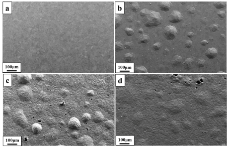
Figure 1. SEM micrographs of pulse plated gold deposits: (a) as- deposited state; (b) after annealing for 3 days at 850ºC; (c) after annealing for 5hours at 900ºC; (d) after annealing for 5 hours at 910ºC.
Electron backscatter diffraction (EBSD) studies of pulse plated gold films
Top view orientation images with inverse pole figures obtained by EBSD technique of as-deposited gold film and annealed at 850ºC for 3 days, 900ºC and 910ºC for 5 hours are revealed in Figure 2a-2d. The average grain size values of the gold deposits determined by the area fraction method available with the TSL software are given in Table 1.
Figure 2a shows EBSD orientation map of as-deposited gold coating consisting of microcrystalline structure with inhomogeneous grains of an average grain size of 6 µm. The EBSD inverse pole figure related orientation maps (color codes are given in the inset of the maps) of the gold deposits annealed at 850ºC, 900ºC and 910ºC for 3 days, 5 hours and 5 hours, respectively are shown in Figure 2b-2d and their average grain sizes are found 7 µm, 9 µm, and 17 µm, respectively. It is observed that the grains are grown slowly in the pulse plated gold layers as the annealing temperature increases. The average grain size of the gold film annealed at 910ºC for 5 hours is more than twice than that of the as-deposited gold film.
The maximum intensity of the texture component of the gold deposits is also given in Table 1 after analyzing the inverse pole figures. From the inverse pole figures, it is found that the microcrystalline gold deposits has a weak <0 0 1>//GD fiber texture before annealing and it became strong <0 0 1>//GD fiber texture after annealing at 910ºC for 5 hours. It is concluded that the maximum intensity of texture component is increasing upon annealing. The grains with a weak <0 0 1>//GD fiber texture of maximum intensity 2.65 and {1 0 0} <0 0 1> texture components are observed in an as-deposited gold film, as shown in Figure 2a. The gold deposit that heated at a temperature of 850ºC for 3 days (Figure 2b) has the grains with the <0 0 1> //GD fiber texture of maximum intensity 3.96 and diluted {1 0 0} <0 0 1> texture components. The strength of the fiber texture component increases a little as compared to the as-deposited gold film due to the minute growth of grains of the as deposited gold film (Figure 2b) having the same <0 0 1>//GD fiber texture. After annealing at 900ºC for 5 hours, the maximum intensity of <0 0 1>//GD fiber texture increases further up to 6.43 (Figure 2c) and the grains have grown further to about 9 µm which also have the <0 0 1>//GD fiber texture. Apart from {1 0 0} <0 0 1> texture component, {1 0 0} <1 1 0> texture component also started appearing in the annealed deposit at 900ºC for 5 hours. The inverse pole intensity of the <0 0 1>//GD fiber texture component in the deposit annealed at 910ºC for 5 hours is 9.79 and <0 0 1>//GD fiber texture component is also generated in the fully grown grains of this annealed gold deposit. The other texture components {1 0 0} <0 0 1> and {1 0 0} <1 1 0> in the annealed deposits became prominent.
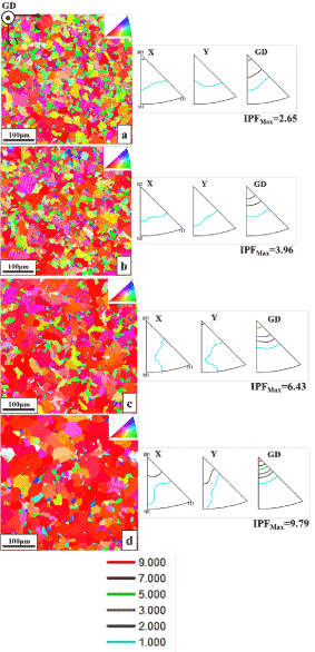
Figure 2. Left: EBSD orientation maps of PED gold deposits: (a) as- deposited state; (b) after annealing for 3 days at 850ºC; (c) after annealing for 5hours at 900ºC; (d) after annealing for 5 hours at 910ºC. Right: Inverse pole figures of the respective gold deposits.
Table 1. Average grain size and maximum intensity of the texture component of the as-deposited and annealed gold deposits.
S.No |
Thermal annealing temperature and time |
Grain Size (microns) |
Maximum Intensity of <0 0 1>//GD Fiber |
01 |
As-deposited gold film |
6 |
2.65 |
02 |
850ºC, 3days |
7 |
3.96 |
03 |
900ºC, 5 hours |
9 |
6.43 |
04 |
910ºC, 5 hours |
17 |
9.79 |
The EBSD orientation maps of the as-deposited and annealed gold deposits with only cube ({1 0 0} <0 0 1>) grains labeled Fuchsia and rotated cube ({1 0 0} <1 1 0>) grains marked yellow are shown in Figure 3a-3d). To know the phenomenon behind the average grain size increase on annealing, the measurements (volume fraction, number of grains and average grain size) on the cube and rotated cube texture components along the growth direction (GD) in both as-deposited and annealed gold films are done by HKL software from EBSD maps, and the results are listed in Table 2. It is noticed that the volume fraction and average grain size of the cube and rotated cube grains increase with increasing annealing temperature whereas total number of grains decreases. The volume fraction and average grain size of both cube and rotated cube grains in an as-deposited gold film are 7.28% and 10 μm; 4.06% and 9 μm, respectively whereas total number of grains is 192 and 167, respectively. The gold deposit annealed at 850ºC for 3 days consists of 8.29% volume fraction, 13 μm average grain size and 144 total number of grains of cube grains as well as 7.6% volume fraction, 11 μm average grain size and 147 total number of grains of rotated cube grains. For the gold film annealed at 900ºC for 5 hours, the volume fraction and the average grain size of cube and rotated cube grains increase to 9.86% and 12%; 16μm and 17 μm while total number of grains decreases to 109 and 132, respectively. The volume fraction and average grain size of cube and rotated cube orientated grains in the gold film annealed at 910ºC for 5 hours are 17.4% and 14.5%; 24 μm and 21 μm respectively while total number of grains are 80 and 72, respectively.
Table 2. Volume fraction and texture indexing of the cube and rotated cube texture component of the as-deposited and annealed gold deposits.
Sample Name |
Cube {100}<001> |
Rotated Cube {100}<011> |
Volume Fraction
(%) |
Total No. of Grains |
Average Grain Size (μm) |
Volume Fraction
(%) |
Total No. of Grains |
Average Grain Size (μm) |
As-deposited gold film |
7.28 |
192 |
10 |
4.06 |
167 |
9 |
850ºC, 3days |
8.29 |
144 |
13 |
7.6 |
147 |
11 |
900ºC, 5 hours |
9.86 |
109 |
16 |
12 |
132 |
17 |
910ºC, 5 hours |
17.4 |
80 |
24 |
14.5 |
72 |
21 |
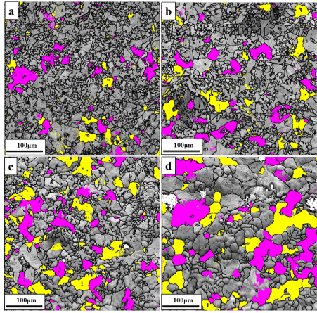
Figure 3. EBSD orientation maps of PED gold deposits with colored cube (marked Fuchsia) and rotated cube (marked Yellow) texture components: (a) as- deposited state; (b) after annealing for 3 days at 850ºC; (c) after annealing for 5hours at 900ºC; (d) after annealing for 5 hours at 910ºC. Note that nearly all grains in all the samples are having <001>//GD fiber texture only.
Figure 1a-1d show the annealing effect on the surface features of the gold film. The as-deposited gold film has smooth surface with inhomogeneous grain structure. The as-deposited gold film is then annealed at elevated temperatures (850ºC for 3 days, 900ºC and 910ºC for 5 hours) which are approximately close to or more than 0.5 times of the melting point of the pure gold material (1077ºC) [22]. As it is expected, in the case of bulk materials, recrystallization occurs at high temperature about 0.5 times of the melting point of the material whereas in case the electrodeposited films, recrystallization may take place at lower temperature depending upon the film thickness, the crystalline grain size, the density and type of defects, the degree of purity and the stress state of the film. Acceleration of diffusion processes and decomposition of the incorporated organic impurities are observed during the recrystallization of the electrodeposits. However, sometimes grain growth is also noticed along with the increase of the porosity upon annealing of the electrochemically deposited films at high temperatures [23].
It could be seen clearly from the SEM analysis of the gold deposit annealed at 850ºC for 3 days (Figure 1b) that beginning of the formation of the hemispherical bulges/bubbles on different places of deposit surface with no porosity and slight growth of the crystallites. The hemispherical bulges/bubbles formation in the annealed gold film is related to the incorporation of impurities such as hydrogen gas in the as-deposited gold film which is reduced generally in parallel with metal deposition during the electrodeposition. In the literature, it is also reported that the gold cyanide complex ions are reduced at very high negative potentials which in turn resulting in the co-deposition of hydrogen ions [24]. Therefore, at this annealing temperature, hemispherical bulges/bubbles are formed due to the trapped hydrogen gas underneath the deposit, trying to evolve out from the deposit surface. The hydrogen gas evolution from the gold and gold alloy electrodeposits upon annealing at different temperatures is explained in detail elsewhere [25]. The similar type of bubbles/swellings formation in the deposit surface is also observed in Cu interconnects prepared by sputtering after annealing at 400ºC in H2/N2 gas atmosphere [26]. From EBSD data of average grain size, it is confirmed that the average grain size increases from 6 μm to 7 μm on annealing of an as-deposited film at 850ºC for 3 days that indicates onset of grain growth. Earlier work also reported that in addition to surface changes, individual grains are grown due to diffusion and accumulation of defects at grain boundaries depending upon the heat treatment temperature [9].
The SEM micrographs of the deposits annealed at 900ºC (Figure 1c) and 910ºC (Figure 1d) for 5 hours reveal the pores formation on both hemispherical bulges/bubbles and remaining places of the gold deposit with grain growth but without cracks. When the film is heated to 900ºC and 910ºC for 5 hours, the pores are started to form throughout the film including on hemispherical bulges/bubbles due to the evolution of trapped hydrogen gas from swellings/bulges. It is also observed that the size of the pores and leveling of the hemispherical bulges/bubbles take place with increasing annealing temperature from 900ºC to 910ºC. Therefore, the surface of the gold deposit annealed at 910ºC for 5 hours is smoother than that of the gold deposit annealed at 900ºC for 5 hours. The leveling of the sharp peaks and edges of the individual grains is noticed from the SEM analysis of the gold films annealed at temperatures higher than 400ºC but 200ºC is the starting temperature [27]. The earlier study also reported that the void formation on the surface of the sputtered Cu deposit with increasing annealing temperature carried out in H2/N2 gas atmosphere due to high internal pressure stored in the bubbles or swellings [26]. The formation of cracks along the grain boundaries of the swellings are also noticed which is similar to that observed in Cu deposits as well as in hydrogen embrittled bulk Cu materials reported in the previous studies [26, 28]. The average grain size increases from 9 μm to 17 μm upon annealing of the as-deposited film from 900ºC to 910ºC for 5 hours.
Generally, the electrodeposited coatings are associated with the fiber texture component, i.e. preferred crystallographic orientation of their grains along the growth direction [29-31]. The as-deposited gold electrodeposit has a weak initial <0 0 1>//GD fiber texture, as shown in Figure 2a. This preferred orientation may have arrived because of the Si substrate’s <100> orientation on which epitaxial growth SiO2 and Au happened. As the annealing temperature increases from 850ºC to 910ºC, it is investigated from their corresponding inverse pole figures (as shown in Figure 2b-2d) that the maximum intensity of <0 0 1>//GD fiber texture is also increased from 3.96 to 9.79. With the increase in annealing temperature the grains are also grown. The newly grown grains also has a <0 0 1>//GD fiber texture component which in turn increased the intensity of the fiber texture. In the <0 0 1>//GD fiber texture, two texture components such as cube and rotated cube ({1 0 0} <0 0 1> and {1 0 0} <1 1 0>) are observed with its volume fraction and grain size is found increased but with decrease in the number of grains with the increase of annealing temperature. From this result, it is confirmed that grain size increase is due to grain growth only and not due to recrystallization. The previous study also reported that the increase of grain size of microcrystalline electrodeposits upon annealing can be resulted by grain growth only rather than by recrystallization which is explained by small amount of stored strain energy in the materials [32]. Sometimes, though the stored strain energy is small the electrodeposits during heat treatment undergo different stages such as recovery, recrystallization and grain growth [33]. Therefore, it is explored that there is a slow increase in the intensity of fiber texture of the gold deposits before and after annealing due to small stored energy which is contributed from the total energy stored in grain boundaries and other defects in the material. As a result, the driving force for grain growth in the gold deposits is low; therefore, the changes in the intensity of the texture component of the gold films are also slow by adding the intensity of the newly grown grains having same fiber texture upon annealing. In literature, it is reported that texture of the electrodeposited films completely changes or sometimes remains unchanged upon annealing due to recrystallization and grain growth of the as-deposited film grains [29-31, 34]. Finally, the presented results showed thermal stability of the gold deposits upon annealing and following the texture changes in them.
In this study, thermal induced changes in microstructure of the gold films fabricated by pulse electrodeposition are investigated by SEM and EBSD techniques. The microstructure analyses of the as-deposited and annealed gold films revealed the smooth surface of the as-deposited film and the formation of hemispherical bulges, pores in the annealed films. The as-deposited gold film shows weak <0 0 1>//GD fiber texture with average grain size of 6 μm. The intensity of the <0 0 1>//GD fiber texture component and grain size is found increased in the gold film with increasing annealing temperatures such as 3 days at 850ºC and 5 hours at 900ºC and 910ºC. In the <0 0 1>//GD fiber texture, the volume fraction, grain size and total number of grains of the two major texture components (cube and rotated cube) are calculated. From the obtained result of the increase in the maximum intensity of texture components with their grain size and decrease in grain numbers of the gold films upon annealing confirmed grain growth phenomenon.
The authors would like to thank the seed grant for research provided by IIT Hyderabad, India.
- Kosaki K, Matsuoka M, Seiwa Y, Orisaka S, Nishitani K and Otsubo M. 1992. Proc. 1st Symp. Electrochem. Microfab. M. Datta, K. Sheppard and D. Snyder (Eds.), PV92-3: 317.
- Williams R (1990) Modern GaAs Processing Methods. Artech House Boston.
- Smallbrugge E, Jacobs B, Falcone S, Geluk EJ, Karouta F (2000) Electroplating of gold using a sulfite-based electrolyte. Proc Symp IEEE/LEOS 143-146.
- Wooten EL, Kissa KM, Yi-Yan A, Murphy EJ, Lafaw DA, et al. (2000) A review of lithium niobate modulators for fiber-optic communications systems. IEEE J Sel Top Quantum Electron 6: 69-82.
- Datta M, Osaka T, Schultze JW (2005) Microelectronic Packaging. CRC Press Boca Raton.
- Holliday R, Goodman P (2002) Going for gold. IEEE Rev 48: 15-19.
- Christie IR, Cameron BP (1994) Gold electrodeposition within the electronics industry. Gold Bull 27: 12-20.
- Todd A (2007) Gold electrodeposition for microelectronic, optoelectronic and microsystem applications. Gold Bull 40: 105-114.
- Raub Ch J, Khan HR, Lendvay J (1976) Temperature-sensitive properties of gold and gold alloy electrodeposits. Gold Bull 9: 123-128.
- Czerwinski F, Szpunar JA (1999) Controlling The Thermal Stability of Texture in Single-Phase Electrodeposits. Nanotruct Mater 11: 669-676.
- Rasmussen AA, Gholinia A, Trimby PW, Somers MAJ (2004) Thermal stability of electrodeposited Ni and Ni-Co layers; an EBSD-Study. Mater Sci Forum 467/470: 1345-1352.
- Amblard J, Froment M, Maurin G, Sakellardiridis P, Spyrellis N (1978) Texture of Materials. Springer. 325-332.
- Czerwinski F, Zielinska-Lipiec A, Szpunar JA (1999) Thermal instability of Ni electrodeposits applied in replication of optical recording devices. Acta Mater 47: 2553-2566.
- Thompson CV, Carel R (1996) Stress and grain growth in thin films. J Mech Phys Solids 44: 657-673.
- Faurie D, Renault PO, Le Bourhis E, Goudeau PH (2006) Study of texture effect on elastic properties of Au thin films by X-ray diffraction and in situ tensile testing. Acta Mater 54: 4503-4513.
- Yeager JD, Bahr DF (2010) Microstructural characterization of thin gold films on a polyimide substrate. Thin Solid Films 518: 5896-5900.
- Dutta I, Munns CB, Dutta G (1997) An X-ray diffraction (XRD) study of vapor deposited gold thin films on aluminum nitride (A1N) substrates. Thin Solid Films 304: 229-238.
- Finot MO, Braybrook GD, McDermott MT (1999) Characterization of electrochemically deposited gold nanocrystals on glassy carbon electrodes. J Electroanal Chem 466: 234-241.
- Hu J, Li W, Chen J, Zhang X, Zhao X (2008) Novel plating solution for electroless deposition of gold film onto glass surface. Surf Coat Technol 202: 2922-2926.
- Mohamed S, El-Deab (2009) On the preferential crystallographic orientation of Au nanoparticles: Effect of electrodeposition time. Electrochim Acta 54: 3720-3725.
- Dey SR, Pfetzing-Micklich J, Brinckmann S, Ehmann M, König D, et al. November 12-13, 2009. Materials for Harsh Environments Bochum (Germany).
- Ercolessi F, Andereoni W, Tosetti E (1991) Melting of Small Gold Particles: Mechanism and Size Effects. Phys Rev Lett 66: 911-914. [Crossref]
- Gamburg YD, Zangari G (2011) Theory and Practice of Metal Electrodeposition. Springer. New York Dordrecht Heidelberg London.
- Sullivan AM, Kohl PA (1997) Electrochemical Study of the Gold Thiosulfate Reduction. J Electrochem Soc 144: 1686-1690.
- Tompkins HG (1975) Diffusion of Cobalt out of Cobalt-Hardened Gold Measured with Auger Electron Spectroscopy. J Electrochem Soc 122: 983-987.
- Konishi S, Moriyama M, Murakami M (2002) Effect of Annealing Atmosphere on Void Formation in Copper Interconnects. Mater T JIM 43: 1624-1628.
- Raub Ch J (1975) The surface structure of gold films. Gold Bull 8: 70-72.
- Koiwa M, Yamanaka A, Arita M, Numakura H (1989) Water in Hydrogen Embrittled Copper. Mater T JIM 30: 991-998.
- Lee DN, Kang S, Yang J (1995) Relationship between initial and recrystallization textures of copper electrodeposits. Plat Surf Finish 82: 76-79.
- Nam HS, Lee DN (1999) Recrystallization Textures of Silver Electrodeposits. J Electrochem Soc 146: 3300-3308.
- Kim I, Sung DY, Park BH, Lee MG (2004) Texture of Electrodeposited Ni Films. Mater Sci Forum 449/452: 565-568.
- Thompson AW, Saxton HJ (1973) Structure, Strength, and Fracture of Electrodeposited Nickel and Ni-Co Alloys. Metall Trans 4: 1599-1605.
- Jacobson BE, Sliwa JW (1979) Structure and Mechanical Properties of Electrodeposited Nickel. Plat Surf Finish 60: 42-47.
- Choi JH, Kang S, Lee DN (1999) Proc. ICOTOM-12. 298. McGill University, Montreal, Canada, 9-13 August, 1999.