Abstract
In2xGa2-2xO3 nanowires were grown at 800°C via the vapor-liquid-solid mechanism on Si(001) using 1 nm Au as a catalyst and by varying systematically the In to Ga ratio. The In2xGa2-2xO3 nanowires have average diameters of » 50 nm, lengths up to 100 mm and consist of a mixture of phases belonging to the cubic bixbyite In2O3 and monoclinic b-Ga2O3. The nanowires exhibited room temperature photoluminescence at 3.1 eV which shifted to the blue upon increasing the content of Ga. In contrast we observe a strong red-shift from 3.1 eV to 1.8 eV after processing under H2S at 700°C due to the diffusion of S into oxygen vacancies and the formation of Ga rich In2xGa2-2xS3. We find that the deposition of Cu over In2xGa2-2xO3 and conversion under H2S between 100°C to 500°C resulted into the formation of Cu(InxGa1-x)S3 nanowires with smaller resistances and a stronger red shift in the photoluminescence from 3.1 eV to 1.5 eV close to the energy gap of Cu(InxGa1-x)S2.
Introduction
Metal oxide (MO) semiconductor nanowires (NWs) such as ZnO [1], SnO2 [2], In2O3 [3], Sn doped In2O3 [4] and Ga2O3 [5] have been investigated and used extensively for the fabrication of nanoscale devices such as sensors, solar cells, photo detectors etc. However the growth and properties of one dimensional ternary oxides such as In2xAl2-2xO3 or In2xGa2-2xO3 have not been investigated widely. Ternary and quaternary oxides like In2xGa2-2xO3 [6] and InGaO3(ZnO)5 (IGZO) [7] have been used as transistors and the backplane of flat panel displays. More specifically In2xGa2-2xO3 is attractive because it has a very low optical absorption coefficient on the order of a few hundreds cm−1 in the visible range, a refractive index of around 1.65 and an energy band-gap of about 3.4 eV. On the other hand the main advantage of IGZO is that it can be deposited in the amorphous phase while retaining a high carrier mobility. One of the main issues concerning the fabrication of nanoscale devices using MO NWs is controlling the surface properties which are necessary to prevent fluctuations in their conductivity due to the adsorption and desorption of oxygen or water. This has been carried out on ZnO and SnO2 NWs using polyimide and poly methyl methacrylate respectively [8,9]. Sulfur passivation has been used to improve mainly the properties of III-V NWs, but recently we investigated the effect of sulfur on the structural, electrical and optical properties of SnO2 NWs and their conversion into SnS2 NWs [10], while we have also shown that post growth processing of Sn doped In2O3 NWs under H2S between 100°C to 600°C resulted into the appearance of band edge photoluminescence (PL) at 3.5 eV close to the energy band gap of In2O3, but no emission in the red or near Infra-Red (IR) [11]. More importantly Cu2SnS3/SnO2 and CuInS2/Sn:In2O3 NWs with ultraviolet PL at 3.7 eV were obtained via the deposition of 60 nm Cu over SnO2 and Sn doped In2O3 NWs and processing under H2S at 500°C [12]. Consequently the sulfur doping of MO NWs may be used to obtain metal oxy-sulfides (MOxS) NWs with different electrical and optical properties similar to β-In2S3-3xO3x [13] which has an optical band gap found to vary from 2.1 eV in pure β-In2S3 to 2.9 eV when it contained 8.5 at.% of oxygen and has been proposed as an alternative to CdS buffer layers in Cu(InxGa1-x)Se2 (CIGS) solar cells. CIGS is a direct band gap semiconductor, with a high light absorption coefficient, and CIGS solar cells exhibit high efficiencies greater than 20%. Hence CIGS/Cu2S core-shell nanowire solar cells (NWSCs) have also been fabricated [14] while Peng et al. [15] prepared CuInSe2 NWs using the vapor–liquid–solid (VLS) mechanism. Similarly Cu(InxGa1-x)S2 is a chalcopyrite material with a near-optimum band gap of 1.5 eV and contains S as opposed to Se which is toxic. However only few efforts have been devoted to the synthesis, properties and application of I–III–VI2 chalcopyrite Cu(InxGa1-x)S2 NWs in solar cells [16].
Considering the above we have carried out a systematic investigation into the growth of In2xGa2-2xO3 NWs via the VLS mechanism by varying the In to Ga ratio but also the effect of S on its properties. The In2xGa2-2xO3 NWs have average diameters of » 50 nm, lengths up to 100 mm and consist of a mixture of phases belonging to the binary constitutent components i.e. the cubic bixbyite crystal structure of In2O3 and monoclinic b-Ga2O3. The In2xGa2-2xO3 NWs exhibited PL at 400 nm or 3.1 eV which shifted to 1.8 eV after post growth processing under H2S well above 500°C due to deep, donor to acceptor transitions and the formation of Ga rich In2xGa2-2xS3. In contrast, we find that the deposition of Cu over the In2xGa2-2xO3 NWs and post growth processing under H2S at lower temperatures between 100°C to 500°C resulted into Cu(InxGa1-x)S2 NWs with smaller resistances compared to the as-grown or S doped In2xGa2-2xO3 NWs and a stronger red shift of the PL that changed from 3.1 eV to 1.5 eV close to the energy band gap of of I–III–VI2 chalcopyrite Cu(InxGa1-x)S2.
Methods
In2xGa2-2xO3 NWs were grown using a low-pressure chemical vapour deposition (LPCVD) reactor consisting of a 1˝ quartz tube, capable of reaching 1100°C, that was fed from a manifold consisting of four mass flow controllers fed with Ar, O2, NH3 and H2. For the growth of the In2xGa2-2xO3 NWs, Sn (Aldrich, 2-14 Mesh, 99.9%), In and Ga (Aldrich, 99.9%) were weighed with an accuracy of ± 1 mg. Square samples of Si(001) ≈ 7 mm x 7 mm were cleaned sequentially in trichloroethylene, methanol, acetone, isopropanol, rinsed with de-ionised water , dried with nitrogen and coated with » 1 nm Au by sputtering. Following this 0.2 g of In and Ga containing a trace of 1 % Sn and the 1 nm Au/Si(001) substrates were loaded inside a quartz boat which was positioned at the centre of the 1˝ tube that was pumped down to 10-4 mBar and subsequently purged with 600 sccms of Ar for 10 min at 1 mBar after which the temperature was ramped up to 800°C using a ramp rate of 30°C/min while maintaining the same flow of Ar. Upon reaching 800°C, a small flow of 10 sccms O2 was added to the main flow of Ar in order to grow the In2xGa2-2xO3 NWs after which the reactor was allowed to cool down without O2. The morphology of the In2xGa2-2xO3 NWs was determined by scanning electron microscopy (SEM) while their crystal structure was determined by x-ray diffraction (XRD) using a Rigaku Miniflex. Subsequently the In2xGa2-2xO3 NWs were exposed to 50 sccm H2S between 100°C to 700°C for 60 min using a ramp rate of 10°C/min in a different reactor capable of reaching 1500°C. All of the In2xGa2-2xO3 NWs were inspected by SEM after exposure to H2S in order to determine changes in morphology, while their crystal structure and phase purity was determined again by XRD. The photoluminescence (PL) spectra of the as grown and S doped In2xGa2-2xO3 NWs on Si(001) were obtained at room temperature using an excitation of 266 nm. Finally we deposited 40 nm of Cu over the In2xGa2-2xO3 NWs and processed these under H2S between 100°C to 500°C after which their properties were determined in the same way as described above. The resistance of the In2xGa2-2xO3 NW networks that were grown on 10 mm x 10 mm quartz and Cu(InxGa1-x)S2 NW obtained after the deposition of Cu and processing under H2S was measured in accordance with O’Dwyer using In contacts [17].
Results and discussion
We will begin with a discussion of the binary oxides, namely In2O3 and Ga2O3, which is necessary to understand the growth and properties of the In2xGa2-2xO3 NWs. We have shown previously that In2O3 NWs with lengths up to » 1 mm and average diameters of » 50 nm can be obtained on 1 nm Au/Si(001) at 700°C and 1 Atm via the reaction of In and O2 [3] but the yield and uniformity was limited up to » 10 mm from the metal sources. In contrast, a significantly higher yield and uniform distribution of Sn doped In2O3 with lengths up to » 100 mm and diameters of » 50 nm were obtained by LPCVD at 800°C on 1 nm Au/Si(001) over distances greater than 10 mm [4]. This is a direct consequence of the larger metal vapor pressure of Sn and In at 10-1 mBar and 800°C. The Sn doped In2O3 NWs grow via the VLS mechanism, have a cubic bixbyite crystal structure, metallic like conductivities and exhibited PL at 2.4 eV while post growth processing under H2S up to 400°C resulted into the emergence of PL at 3.5 eV due to band edge emission from In2O3 but no PL in the red or near infra red (IR) [11]. Similar to the case of In2O3 the reaction of Ga with O2 at 900°C and 1 Atm lead to the growth of b-Ga2O3 NWs on 1 nm Au/Si(001) but the yield and uniformity was not satisfactory. The b-Ga2O3 NWs had a monoclinic b-Ga2O3 crystal structure and exhibited PL with a maximum at 520 nm or 2.4 eV attributed to oxygen vacancies and states lying energetically in the upper half of the energy band gap of b-Ga2O3 as shown by ultrafast absorption-transmission spectroscopy [18]. A higher yield and uniform distribution of Sn doped Ga2O3 NWs was obtained by LPCVD at 800°C and 1 mBar. The Sn doped Ga2O3 NWs had a monoclinic crystal structure and exhibited PL at 3.5 eV while post growth processing under H2S above 500°C resulted into the emergence of PL at 1.8 eV. This red emission from the b-Ga2S3 NWs was attributed to deep donor to acceptor transitions and was exploited for improving the efficiency of a Si solar cell via spectral shifting [19].
Here we have grown Sn doped In2xGa2-2xO3 NWs by LPCVD at 800°C and 1 mBar using Sn , In and Ga metal sources containing 13, 30, 35, 40, 50, 70, 75 % Ga and only 1% Sn. The vapor pressures of In and Ga at 800°C are » 10-4 and 10-5 mBar respectively while In and Ga have similar ionic radii which renders feasible the compositional tuning of In2xGa2-2xO3 NWs. We obtained a high yield and good uniformity of In2xGa2-2xO3 NWs with average diameters of » 50 nm and lengths up to 100 mm. A typical SEM image is shown in Figure 1a. We find that the In2xGa2-2xO3 NWs do not grow on plain Si so one dimensional growth occurs via the VLS mechanism, as depicted schematically in Figure1b, similar to Sn doped In2O3 where it has been shown that the Au nanoparticles at the top of the Sn doped In2O3 NWs are in fact rich in Sn not In [20]. The In2xGa2-2xO3 NWs exhibited clear peaks in the XRD as shown in Figure 2 from which they appear to consist of a mixture of phases belonging to the binary constituent components i.e. the cubic bixbyite crystal structure of In2O3 and monoclinic b-Ga2O3. There are few reports on the synthesis of pure In2xGa2-2xO3 and the highest conductivities have been obtained using Sn as a dopant [21]. Solid solutions of In2xGa2-2xO3, where x < 0.4, has been shown to result in indium substitution into the β-Ga2O3 lattice, while x > 0.95, results in gallium substitution into the cubic In2O3 lattice. For 0.4 < x < 0.95 phase segregation occurs and results in β-Ga2O3 and an In2O3-Ga2O3 phase with the cubic In2O3 structure [22]. It is worthwhile pointing out that the structural, electronic, and optical properties of In2xGa2-2xO3 have been determined recently by hybrid density functional methods and it has been shown that the structure of In2xGa2-2xO3 is similar to β-Ga2O3 but it is distinct from Ga doped In2O3 [23]. We find that the XRD spectra of the In2xGa2-2xO3 NWs obtained using 25 to 70% Ga contain a few weak, but nevertheless well resolved peaks, that do not belong to In2O3 or b-Ga2O3 as shown in Figure 2 but must belong to a Ga rich In2xGa2-2xO3 phase since they do not correspond to SnO2. Before elaborating further, it is worthwhile pointing out that we tried to grow In2xAl2-2xO3 NWs via the VLS mechanism but we found from high resolution XRD that the Al was not incorporated in the crystal lattice of In2O3 due to the large difference in the ionic radii of Al and In but also due to the fact that Al has a very large affinity to oxygen which is known prevent one dimensional growth via the VLS mechanism [24]. Besides we did not observe a mixture of In2O3 and Al2O3 phases in the XRD and did not detect more than 1% Al by energy dispersive x-ray analysis (EDX) which is different to the case of the In2xGa2-2xO3 NWs. A typical EDX spectrum obtained from the In2xGa2-2xO3 NWs obtained with 25% Ga is shown in Figure 1c from which we observe distinct peaks belonging to In and Ga. This clearly shows that the In and Ga are incorporated in the In2xGa2-2xO3 NWs while the % at. content of In and Ga in the In2xGa2-2xO3 NWs obtained using metal sources containing different ratios of In to Ga is shown as an inset in Figure 1(c). It is evident that one may tune the actual composition of the In2xGa2-2xO3 NWs over a broad range in contrast to the case of In2xAl2-2xO3 NWs. These findings are similar to the case of Sn doped In2O3 NWs where we showed that it is possible to tune the crystal structure from cubic bixbyite In2O3 to tetragonal rutile SnO2 via a regime consisting of a mixture of In2O3 and SnO2 [4]. Recently we showed that the same is also true for Sn doped Ga2O3 NWs. Both Sn doped In2O3 and Sn doped Ga2O3 NWs were grown by LPCVD at 800°C and 1mBar which are exactly the same growth conditions used for the growth of the Sn doped In2xGa2-2xO3 NWs. The ability to tune the composition of the In2xGa2-2xO3 NWs is attributed to the fact that its constituent binary oxide components can be grown using exactly the same growth conditions and Sn as a dopant but also due to the similar ionic radii of In and Ga. A schematic illustration of the VLS growth mechanism is shown for completeness in Figure 1b. All of the In2xGa2-2xO3 NWs showed PL with a maximum between 350 nm to 400 nm as shown in Figure 3a and a tail extending to 500 nm which is attributed to the existence of oxygen vacancies and states lying energetically in the upper half of the energy band gap of the In2xGa2-2xO3 NWs, as shown previously using ultrafast absorption transmission spectroscopy in the case of the b-Ga2O3 or In2O3 MO NWs. Interestingly we find that the PL of the In2xGa2-2xO3 NWs grown using more than 30 % Ga is slightly blue shifted, which is consistent with a change in the composition of the In2xGa2-2xO3 NWs from In to Ga rich and results into an increase in energy band gap. More specifically the PL has a maximum at 400 nm or 3.1 eV for 10 to 30% Ga but shifts to 350 nm or 3.5 eV above 30% Ga which is close to the experimental energy band gaps of bulk In2xGa2-2xO3.
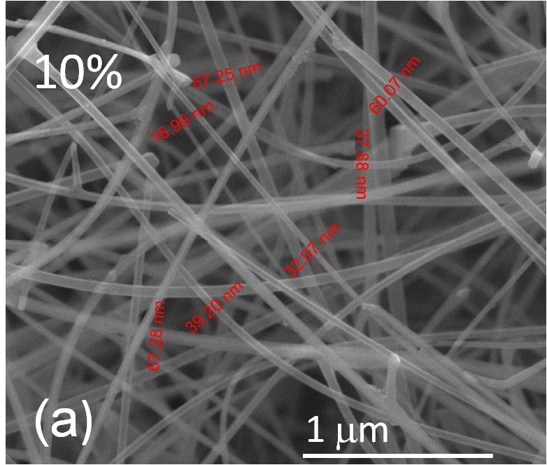
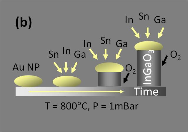
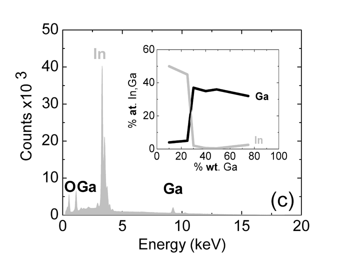
Figure 1a. SEM image of the In2xGa2-2xO3 NWs obtained with 25 wt. % Ga (b) corresponding EDX spectrum of In2xGa2-2xO3 with 25% Ga ; inset shows variation of the % at. In and Ga in the In2xGa2-2xO3 NWs versus the ratio of Ga to In metal sources (c) schematic diagram of the VLS growth mechanism for one dimensional growth of the In2xGa2-2xO3 NWs.
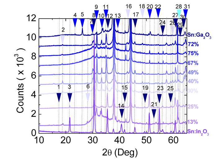
Figure 2. XRD of In2xGa2-2xO3 NWs grown using 13, 25, 30, 40, 49, 67, 72 and 75% Ga. Also shown for comparison of Sn doped In2O3 (bottom trace) and Sn doped Ga2O3 (top trace ). The peaks have been labeled for clarity with arrows in ascending order and increasing angle as follows : 1►17.54°(010)In2O3, 2►18.84°In2xGa2-2xO3, 3►21.44°(022)In2O3, 4►23.44°(012)Ga2O3, 5►26.20°(-012)Ga2O3, 6►28.06°In2xGa2-2xO3, 7►29.78°(400)Ga2O3, 8►30.56°(200)In2O3, 9►31.30°(002)Ga2O3, 10►33.06°(101)Ga2O3, 11►35.04°(111)Ga2O3, 12►35.46°(400)In2O3, 13►39.42°(-112)Ga2O3, 14►40.66°(332)In2O3, 15►41.82°(422)In2O3, 16►42.98°In2xGa2-2xO3, 17►45.68°(134)In2O3, 18►48.50°In2xGa2-2xO3, 19►49.26°(600)In2O3, 20►51.42°(12)Ga2O3, 21►52.80°(433)In2O3,22►54.32°(-113)Ga2O3, 23►54.74°(611)In2O3, 24►56.20°(026)In2O3, 25►59.12°(622)In2O3, 26►59.74° In2xGa2-2xO3,27►60.07°(136) In2O3, 28►62.04°(301)SnO2 , 29►62.58°In2O3 (444) 30►63.58°(543)In2O3, 31►64.34°(121)Ga2O3. The peaks belonging to Sn doped In2O3 are labeled with dark blue ► arrows and those of Sn doped Ga2O3 with ► blue. A few weak but well resolved peaks appear to belong to a Ga rich In2xGa2-2xO3 are labelled with lighter color. Only one peak has been identified as belonging to SnO2.
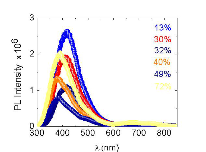
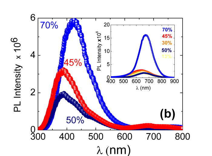
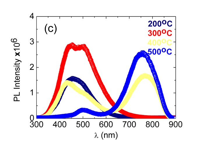
Figure 3a. Room temperature PL of as-grown In2xGa2-2xO3 NW obtained using different % Ga content metal source (b) Room temperature PL of In2xGa2-2xO3 NWs after processing under H2S at 500°C ; inset shows the PL after processing under H2S at 700°C (c)PL of chalcopyrite Cu(InxGa1-x)S3 NWs obtained by deposition of 40 nm Cu over the In2xGa2-2xO3 NWs grown using 30% Ga and processing under H2S at 200°C, 300°C, 400°C and 500°C.
The In2xGa2-2xO3 NWs were further processed under H2S at 500°C, 700°C and 900°C in order to determine their optical properties before the deposition of Cu and their conversion to Cu(InxGa1-x)S3 NWs. It is known that H2S undergoes complete decomposition on the surface of oxides, even at room temperature, and the S atoms bond to the metal cations of the surface. The ionic radii of O2− and S2− are 1.32 Å and 1.82 Å respectively meaning that S will also diffuse into the In2-xGaxO3 and hence S2− will substitute O2− or fill in vacancies. We find that the In2-xGaxO3 NWs processed under H2S at 500°C showed PL at 3.5 eV but a red shift occurred to 1.8 eV following processing at 700°C and 900°C as shown in Figure 3b which is similar to the case of Sn doped Ga2O3 NWs. This red emission is attributed to deep donor to acceptor state recombination similar to what has been observed by in the case of two dimensional Ga2S3 [25]. One may observe in fact, that the PL intensity of the S doped In2-xGaxO3 NWs, becomes stronger with increasing Ga content, suggesting that the red emission is related to the formation of b-Ga2S3 [19]. All of the S doped In2-xGaxO3 NWs had very high resistances, in excess of 100 MΩ consistent with the high resistances measured in the case of Ga2S3 [25]. However we find that the deposition of 40 nm Cu over In2-xGaxO3 NWs and post growth processing under H2S at 100°C, 200°C, 300°C, 400°C and 500°C resulted into Cu(InxGa1-x)S2 NW networks with smaller resistances of the order of 100 kΩ. More interestingly we find that the PL shifts from 3.1 eV to 1.55 eV after processing at 500°C, as shown in Figure 3c, which is different to the case of the plain In2-xGaxO3 NWs that exhibit PL at 3.1 eV after processing under H2S at 500°C. Note also that the PL of the In2-xGaxO3 NWs has a maximum at 1.8 eV after processing at 700°C so the emission at 1.55 eV is most likely related to the formation of chalcopyrite Cu(InxGa1-x)S2 which has an energy band gap of 1.5 eV. We found that the Cu(InxGa1-x)S2 NWs obtained from In2-xGaxO3 NWs with 30% Ga have a completely different XRD pattern compared to the S doped In2-xGaxO3 NWs, both of which were processed at 500°C. This is similar to the formation of CuInS2 which we observed recently following the deposition of Cu over Sn doped In2O3 NWs and post growth processing under H2S at 500°C [12]. In effect the Cu and S will diffuse and react with the In2-xGaxO3 NWs at elevated temperatures. Lower temperatures do not favor the diffusion of Cu and S so the PL has a maximum at 450 nm to 500 nm but the resistance of the resultant Cu2S/In2-xGaxO3 core-shell NW networks was of the order of a few Ω.
Conclusion
We have grown In2xGa2-2xO3 NWs at 800°C via the VLS mechansism on Si(001) using Au as a catalyst and varied systematically the In to Ga ratio. The In2xGa2-2xO3 NWs have average diameters of » 50 nm, lengths up to 100 mm and consist of a mixture of distinct phases belonging to cubic bixbyite In2O3 and monoclinic b-Ga2O3. All In2xGa2-2xO3 NWs exhibited room temperature PL at 400 nm or 3.1 eV which shifted slightly to the blue upon increasing the content of Ga. In contrast we observed a strong red-shift in the PL from 3.1 to 1.8 eV after post growth processing under H2S above 500°C which is attributed to the formation of Ga rich In2xGa2-2xS3. More importantly the deposition of Cu over the In2xGa2-2xO3 NWs and post growth processing under H2S at lower temperatures between 100°C to 500°C resulted into I–III–VI2 chalcopyrite Cu(InxGa1-x)S3 NWs with smaller resistances compared to the as-grown and S doped In2xGa2-2xO3 NWs but also a stronger red shift of the PL from 3.1 to 1.5 eV which is close to the energy band gap of Cu(InxGa1-x)S3.
References
- Law M, Greene LE, Johnson JC, Saykally R, Yang P (2005) Nanowire dye-sensitized solar cells. Nanowire dye-sensitized solar cells.Nat Mater 4: 455-459. [Crossref]
- Tsokkou D, Othonos A, Zervos M (2012) Carrier dynamics and conductivity of SnO2 nanowires investigated by time-resolved terahertz spectroscopy.ApplPhysLett 100: 133101.
- Tsokou D, Zervos M, Othonos A (2009) Ultrafast time-resolved spectroscopy of In2O3 nanowires. J ApplPhys106: 084307.
- Zervos M, Mihailescu, Giapintzakis J, Othonos A (2014) Broad compositional tunability of indium tin oxide nanowires grown by the vapor-liquid-solid mechanism. ApplPhysLettMat 2: 056104.
- Lopez I, Castaldini A, Cavallini A, Nogales E (2014) J Phys D ApplPhys 47: 415104.
- Presley R, Hong D, Chiang H, Hung C, Hoffman R, et al (2006) Transparent ring oscillator based on indium gallium oxide thin-film transistors.Sol Stat Elect 50: 500.
2021 Copyright OAT. All rights reserv
- Nomura K, Ohta H, Ueda K, Kamiya T, Hirano M, et al. (2003) Thin-film transistor fabricated in single-crystalline transparent oxide semiconductor. Science 300: 1269-1272.[Crossref]
- Huh J, Joo MK, Jang D, Lee JH, Kim GT, (2012) Reduced charge fluctuations in individual SnO 2 nanowires by suppressed surface reactions. J Mater Chem22: 24012.
- Park WI, Kim JS, Yi GC, Bae MH, Lee HJ (2004) Fabrication and electrical characteristics of high-performance ZnOnanorod field-effect transistors. ApplPhysLett85: 5052.
- Abat C, Desboves G, Olaitan AO,Chaudet H, Roattino N, et al. (2015) Increasing burden of urinary tract infections due to intrinsic colistin-resistant bacteria in hospitals in Marseille, France.Int J Antimicrob Agents 45: 144-150.[Crossref]
- Zervos M, Mihailescu CN, Giapintzakis J, Othonos A, Travlos A, et al. (2015) Electrical, structural, and optical properties of sulfurized Sn-doped In2O 3 nanowires. Nanoscale Res Lett10: 995.[Crossref]
- Karageorgou E,Zervos M, Othonos A (2014) Sulfur doping of M/In2O3 (M= Al, W) nanowires with room temperature near infra red. PhysLettMat 2: 116107.
- Barreau N,Marsillac S,Albertini D,Bernede J (2002) Structural, optical and electrical properties of β-In 2 S 3-3x O 3x thin films obtained by PVD.Thin Solid Films 403: 331.
- Inguanta R,Livreri P,Piazza S,Sunseri C (2010) Electrochem Sol Stat Lett13: 22.
- Peng H, Schoen DT, Meister S, Zhang XF, Cui Y (2007) Synthesis and phase transformation of In(2)Se(3) and CuInSe(2) nanowires. J Am ChemSoc129: 34-35. [Crossref]
- Chen LZ,LiaoJD,Chuang YJ (2011) Synthesis and characterization of chalcopyrite quaternary semiconductor Cu (In x Ga 1− x) S 2 nanowires by electrospun route.Thin Solid Films519: 3658.
- O'Dwyer C, Szachowicz M, Visimberga G, Lavayen V, Newcomb SB, et al. (2009) Bottom-up growth of fully transparent contact layers of indium tin oxide nanowires for light-emitting devices. Nat Nanotechnol4: 239-244.[Crossref]
- Othonos A,Zervos M,Christofides C (2010) Carrier dynamics in β-Ga2O3 nanowires. Journal of Applied Physics108: 124302.
- Othonos KM, Zervos M, Christofides C, Othonos A (2015) Ultrafast Spectroscopy and Red Emission from β-Ga2O 3/β-Ga 2S 3 Nanowires. Nanoscale Res Lett10: 1016.[Crossref]
- Gao J,Chen R,Li DH,Jiang L,Ye J, et al.(2011) UV light emitting transparent conducting tin-doped indium oxide (ITO) nanowires.Nanotechnology22: 195706.
- Phillips JM,Kwo J,Thomas GA,Carter SA (1994)Transparent conducting thin films of GaInO3.ApplPhysLett 65: 115.
- Edwards DD,Folkins P,Mason T (1997) Phase Equilibria in the Ga2O3In2O3 System. J AmerCerSoc80: 253.
- Wang V,Xiao W,Ma DM, Liu RJ, Yang CM (2014) Structural, electronic, and optical properties of GaInO3: A hybrid density functional study. J ApplPhys115: 043708
- Zervos M,Mihailescu C,Giapintzakis J,Othonos A (2015) Sulfur doping of M/In2O3 (M= Al, W) nanowires with room temperature near infra red emission. AIPAdvances 5: 097101.
- Ho CH, Chen HH (2014) optically decomposed near-band-edge structure and excitonic transitions in Ga2S3.Scientific Reports 4: 6143.