The purpose of this review is to create a high density Nanopattern using Nanosphere Lithography which can be used in photonics application, sensors or electronics industry.
There are several ways to create high density Nanopatterns using Nanolithography. Nanolithography involves the use of colloids which are deposited on a flat substrate using several different techniques such as spin coating, dipcoating, Langmuir Blott Technique and Template Directed Colloidal Self Assembly. The technique that leads to the best results are the ones that lead to an ordered structure on a larger scale through the template directed colloidal self assembly. Therefore when it comes to designing a high density Nanopattern it is better to use the template directed colloidal design.
If one wants a specific pattern there are several different techniques one can use to achieve a nanopattern with a specific design. This is done by further tailoring the polystyrene spheres through Metal dot catalyzed CVD, Selective etching Solution growth, On sphere gas phase deposition, Shadowed oblique angle deposition etc. With each of these techniques different patterns can be achieved such as a hexagonal closed pack array, Nanogaps, Nanochain etc.
This review analyzes how one should make a high density nanopattern. It will go through several ways to allow for the colloidal crystal layer to be deposited on a flat substrate. The review will include the best way to allow for an ordered colloidal layer to be deposited on a substrate on a large scale with few grain defects. The review will then determine different ways to tailor this ordered colloidal layer into structures of various designs depending on the design one needs to create.
One dimensional nanostructures are considered to be the essential components for the next electronics, photonics, sensors, electrochemical and energy applications. In the past, synthesis of one dimensional nanostructure was due to numerous techniques including vapour phase transport, chemical deposition, solution processes, pulsed laser deposition, template assist process etc. With the use of these techniques unique applications in sensors, transistors, light emitting diodes, nanogenerators, batteries and solar cells have been created. The full potential of nanostructures can be unleashed only when one is able to synthesize nanoscale building blocks but also to assemble them into various different patterns and in a controlled way. Some of the potential applications are for energy storage, the enhancement of the capacity and rate capability in lithium-ion batteries and light coupling and electron lifetime in dye sensitized solar cells. One dimensional nanosphere arrays can also be used in photonics; ordered arrays can be high refractive index columns in air, making them a replacement for two dimensional photonic crystals [1]. In bio and life sciences the pitch between nanopillars could influence cell adhesion.
Although many applications use one dimensional array one of the foremost challenges is to assemble these nanoarray structures into an ordered pattern so that the full potential of nanoarrays can be entirely extracted.
In order to get an ordered one dimensional array nanopatterning techniques are required to control the size, spacing, shape and orientation and to allow high throughput, large area and low cost. Up until now the method to create an ordered one dimensional array has been through producing a pattern of a nanoarray on substrates which include optical or electron beam lithography, nanoimprinting, self assembly and template assisted processes [1]. In the methods mentioned above electron beam lithography offers control over the size, spacing and shape of nanostructures. However, equipment costs are high, resist materials, must be used, throughput is low due to a long exposure time leading to a complex process [1].
The most prominent patterning method is template based synthesis. There are two types of templates, hard templates and soft templates. Hard templates have a good ability to produce complex one dimensional structures and have good control of the size, dimension and composition of the array. A problem with hard templates is the ability to remove templates after synthesis and keep a uniform morphology of the arrays. Soft templates consist of organic surfactants, polymers, and even biological viruses which are flexible in shape. The nanostructures in these cases tend to be polycrystalline and may aggregate into bundles which lead to an unordered structure [1].
Recently self assembled colloidal crystal monolayers composed of polystyrene spheres or silica have been used to fabricate ordered arrays with well defined nanostructures because of their flexibility and controllable parameters [1]. For the most part these templates are in hexagonal closed packed or non-close packed pattern on substrates which can be used for surface enhanced Raman scattering, antireflective coating, photonic crystals and as flexible templates to fabricate one dimensional nanostructure arrays. The structure of these arrays can be tuned by changing the diameter of the polystyrene of the polystyrene spheres and experimental conditions. The size and shape of the nanopillars can be controlled by the size and shape of the sputtered aluminum mask, which are determined by the feature size of the polystyrene sphere mask and the number of colloid layers. Nanopillars with different shapes can also be fabricated by adjusting the RIE conditions such as gas species, bias voltage and exposure period for an aluminum mask with a given shape.
The one dimensional nanoarrays produced can be used in a variety of applications for e.g. field emitters, photonic crystals, antireflection, wetting surface etc.
A colloid can be defined as a mixture in which finely divided particles are dispersed in another substance. This could be gaseous, liquid or solid, colloids range in size between nanometers and micrometers. One of the interesting properties that colloids have is the spontaneous formation of periodic particle arrays called colloidal self assembly. In certain conditions, particles can be arranged regularly, in close packed structures forming colloidal crystals. In most cases polystyrene, PMMA (polymethyl methacrylate) or silica colloidal spheres are used for good quality colloidal crystal lattices. These nanosphere arrays can be used as lithographic masks and t techniques are called nanosphere lithography [2].
Polymer particles with narrow size distributions such as polystyrene and PMMA beads with narrow size distribution can be synthesized with suspension, emulsion, dispersion and precipitation polymerizations. Emulsifier free emulsion polymerization has been widely used because of the surface properties of the polymeric latexes are controlled by an initiator or comonomers in the absence of an emulsifier [3]. This helps to simplify the synthesis procedure. During this process the reaction temperature and monomer concentration are the most important factors that control the size of the polymer beads. The solubility of the monomer in the aqueous phase depends on the temperature and the depletion time of the monomer varies with monomer concentration, the particle size decreases with an increase in temperature and with a decrease in monomer concentration. The size of the polymer beads that are formed are in the range of 100-700nm using emulsifier free polymerization [2]. If the particle size needed is greater than one micrometre a single step dispersion polymerization is used. The reaction site is a monomer droplet stabilized with a surfactant and imitator which is soluble in oil and diffuses the monomer droplets.
For inorganic metal oxide particles e.g. silica particles, can be prepared using sol gel chemistry , in this case the size and polydispersity of the particles are related to pH values, concentration of the catalyst, composition of the reagent, type of solvent and reaction temperature. The sizes of the silica particles that can be formed are between 200-600nm [1]. If larger silica particles are necessary a seeded growth technique can be used.
Dip coating
The dip coating method involves pulling up a substrate that is immersed in a colloidal suspension. One can deposit a uniform monolayer of colloidal particles on a large wafer. The dip coating method uses capillary force and controlled evaporation to induce colloidal self organization. The quality of the ordered arrays is determined by the evaporation rate, the evaporation rate can be controlled by a step motor which helps lift up the wettable substrate from the colloidal suspension at a slow rate (Figure 1).
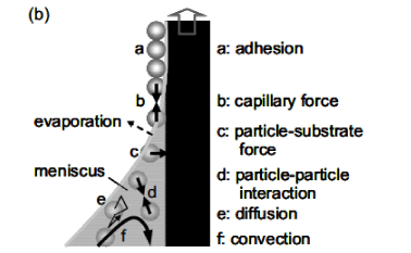
Figure 1. Dip Coating Method [2]
Spin coating
Spin Coating is a technique where the colloidal suspension is spin coated onto a substrate which accelerates solvent evaporation and colloid aggregation. During the centrifugal spreading of a suspension onto a wettable substrate the colloid particles organize themselves into a hexagonal array more rapidly in comparison to evaporation methods such as dip coating. The thickness of the particle layer is due to the particle loading and also the spin speed. The Spin coating methods is also advantageous because it can be used for mass production because the process is rapid and compatible with wafer scale processes which are well established in the area of photolithography.
After the development of the dip coating method, most self assembly of colloid arrays have focused on enhancing the quality, productivity, and controllability of self assembled structures. Various methods have been created to reduce grain boundaries, dislocations, vacancies and variations of the thickness of the colloid layers with a simple and rapid process [1]. Self assembly at the air/liquid or oil/liquid interface, deposition of particles using electrophoresis and template assisted self assembly were applied to fabricate two dimensional colloid arrays with lower defect densities.
Electrophoretic deposition
Electrophoretic deposition of colloidal particles is another way to deposit colloidal suspension onto a substrate. Electrophoretic deposition of particles uses the movement of particles that is driven by an electrical field. Particle assembly happens inside a thin layer of a colloidal suspension sandwiched by conducting substrates such as indium tin oxide coated glass slide [3]. Electrophoretic movement not only accelerates the sedimentation speed of small colloids but also guides the growth of a colloidal crystal over a large area in a controlled manner [3].
Langmuir blodgett
Another method is the Langmuir Blodgett method in which surface modified colloidal spheres are trapped at the air liquid interphase. Using the Langmuir Blodgett coating process they can be transferred onto a substrate forming a dense monolayer of colloidal spheres. Transferring the pattern onto a substrate is challenging but can be done through a combination of chemical modifications to a liquid bath and control of the transfer rate [4]. First the colloidal mixture in water is mixed with ethanol and a small amount of polyethylene oxide (PEO) powder creating a solution with lower density than water that spreads across the surface. The PEO serves to bind the particles together as they assemble creating a robust monolayer during the transfer [4]. A 3:2 ratio of ethanol to solution can be used with a 4 wt% colloidal solution [4]. The solution is sonicated and then distributed on a wetted glass surface forming a monolayer of nanoarrays. Once the monolayer is formed it is transferred to a submerged substrate by draining the water bath. The rate by which the monolayer is transferred is controlled by placing the substrate on an aluminum block with a ten degree angle and a small notch to hold the substrate in place while the bath is drained. The draining speed is controlled by a flow nozzle so that the contact angle. The transfer can be to either a hydrophobic or hydrophilic surface. However, faster transfer is onto a hydrophilic surface e.g. glass.
Colloidal crystal layers deposited onto flat substrates contain domains. Domain sizes depend on materials and methods used for deposition. A crystal domain of tens of micrometers in length with some defects can typically be found in two dimensional self assembly of monodispersed polystyrene or silica nano spheres of a few hundred nanometers in diameter. In close packing, periods of sphere arrays are determined by their diameter. To obtain higher areal density patterns, smaller spheres are necessary as building blocks. However, polystyrene or silica nano spheres show smaller colloidal crystal domain sizes. In dip coating using colloidal silica below 100nm in diameter, one finds cracks and defects in colloidal lattices. In spin coating one cannot find cracks in the lattice until the colloidal polymer nano sphere is smaller than 50nm. Considering this information for high density nano patterning, a more sophisticated technique is needed to control the domain sizes of colloidal crystals, crystal orientations and ordering patterns.
Template assisted self assembly
In the absence of designed patterns a colloidal monolayer shows a short range of attraction of the electrolyte but with a long range disorder. Template assisted self assembly removes this problem. Template assisted self assembly of colloidal particles is employed for suppressing defect formation of colloidal crystals. The deposition of colloids on a substrate usually takes place with chemicals or charges on a physically patterned substrate. The topography of the substrate can confine the self assembly of particles and the ordering quality and stacking sequence can be controlled by changing the ratio of the particle size to the feature size of the patterned geometry. It has been verified that colloidal crystals have been grown on V-shaped grooves as well as chemical or charge contrast on substrates patterned with self assembled mono layers or poly electrolytes can induce the arrangement of colloidal particles into a set pattern. However, most of the tests have been done on 100nm spheres. Sub 100nm particles, such as 40nm gold nanospheres and 40nm and 70nm silica nanospheres have not shown long range order when deposited on large pre patterns. This shows that for sub 100nm spheres much smaller template structures must be used (Figure 2).
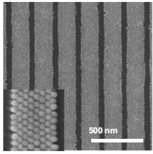
Figure 2. Directed Self Assembly of Silica Nanospheres on a patterned substrate [2]
Design discussion
The best method for forming a nanopattern is the Template Assisted method. It allows for a long range order unlike dipcoating and spin coating. It also supresses defect formation of colloidal crystals. Due to the topography of the substrate one can confine the self assembly of particles and the ordering quality and stacking sequence can be controlled by changing the ratio of particle size to feature size of the patterned geometry. The long ordered nanopatterned can be tailored to form particle structural shapes by different methods which can be found below.
Tailoring the final nanoarray product
The final nanoarray product can be tailored based on different techniques such as CVD growth, solution growth, oblique angle deposition and selective etching.
Metal dot-catyzed CVD-honey comb lattice
With good uniformity and high order , Polystyrene sphere colloidal crystals make good templates for fabricating large area metal catalyst arrays. When one combines PS template directed metal of arrays and CVD growth the result is the formation of one dimensional nanoarrays. After the selfassembly of the PS nanospheres on a surface a gold film is deposited on the nanospheres. This forms a coating of gold on the upper hemispheres and a gold dot array on the substrates by penetrating a beam through the spaces between the PS spheres. A pre coating of PS nanospheres can narrow the holes between the spheres and therefore decrease the dot size. This creates growth of nanowires on individual gold dots. The nanowires form a honeycomb lattice which is the same pattern as the gold nanodots. These nanowires exhibit high degrees of ordering and are well separated (Figure 3).
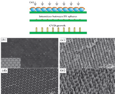
Figure 3. Metal dot-catyzed CVD analysis and the resulting nanoarray [1]
Selective etching
Another way to make nanoarrays is through selective etching. In this method PS sphere monolayers act as a mask for selective etching of thin films or bulk materials. A PS sphere monolayer can be combined with wet etching through a solution chemical reaction or dry etching.
For chemical etching, monolayers of PS spheres are self assembled on a silica substrate, the diameter of the PS spheres is reduced by RIE. This leads to the formation of colloidal particle arrays that are no longer closed packed. A silver film is then thermally evaporated onto the PS silica spheres as a catalyst. The silver film is porous due to the PS mask and has a hexagonal array of holes. During etching the silver film catalyzes the etching of silica beneath it. The walls of the honeycomb are etched away and the remnant silica forms a nanowire array. The PS spheres are removed by dissolution in a chemical and the silver film is dissolved in boiling aqua regia. The resulting nanoarrays are homogeneously distributed on the substrate over a large area. The mean diameter of the wires can be controlled by selecting PS spheres with the desired diameter. The length of the nanowire can be controlled by the duration of the etching process.
For dry etching, PS sphere formed metal dot arrays can be used as a mask for controlled dry etching fabrication of Silica one dimensional structure arrays through RIE. This forms triangular dot arrays with a hexagonal order. By varying the percentage of oxygen in mixed etching gases the size and morphology of silica nanopillars can be tuned. The base width of the nanoarray increases with the percentage of oxygen. The height/base ratio decreases with oxygen content as its percentage reaches about twenty percent. The way that this process takes place is PS is spin coated onto a substrate of silica, RIE with oxygen is used to tailor the size of the PS spheres, and deep RIE of Si is used to etch the pillar structure. This process can produce silica structures with an aspect ratio of up to 40 or more [1].
Solution growth
Due to the low temperature during solution growth the PS monolayer is facile in the process of electrochemical deposition, hydrothermal growth and chemical deposition [1]. Electrodeposition is a useful technique for nanowire growth within a large area. The deformation of a PS monolayer can be introduced to control the patterned nanorod arrays. A PS monolayer is self assembled on a substrate through spin coating, and then different degrees of template deformation are introduced under heating near the glass transition temperature. Finally, electrochemical deposition is implemented on these deformed PS monolayer covered substrates. Since the array pattern is confined by the shape and pattern vacancies within a template the nanowire density and uniformity of the formed arrays can be adjusted [1]. When a PS monolayer template is heated the growth of well separated short nanorods are formed due to the deformation driven separation of voids in the template. However if the deformation is excessive some voids in the template vanish due to PS fusion resulting in the absence of nanorods in this site. As the heat treatment is increased to one minute the nanorod separation becomes obvious and to 1.5 minutes template eating the separation of the nanorods is further profound [1]. This adjustment of local spacing is significant for the arrays field emission performance when one considers the screening effect during electron emission [1]. In this technique the method utilizes deformed tailored colloidal monolayers and electrochemical deposition at temperatures as low as 70 ͦC without the need of catalysts or performed seed layers [1]. This method is cheap and can be used to produce large scale arrays.
Another way to form nanotubes using a PS monolayer is coating a substrate with ZnO seed layers, followed by deposition of PS colloids. A hydrothermal process is used to grow one dimensional ZnO nanostructures on the substrates patterned with PS colloid monolayers. This results in the growth of ZnO tubular structures just below the PS colloids and solid nanorods at the apertures between adjacent spheres.
On sphere gas phase deposition
In this type of deposition the top part of a PS monolayer is used to fabricate one dimensional nanoarray with an hncp arrangement. This is done by fabricating PS monolayer colloidal crystals on a silica substrate by spin coating. The substrate with a colloidal monolayer is placed in a chamber for PLD (pulsed laser deposition) in an off axis configuration to the target. The sample is then put into an oven for heating in air. The result is an ordered and well structured array with an hncp arrangement. The array is formed and is heated . When the substrate and colloidal structure is heated the PS spheres are changed to a polycrystal and moved vertically down to the original positions of the PS spheres. The nanorod decreases during this process and an hncp hierarchical nanorod array is formed from the pre-existing hncp amorphous array. The resultant film adhered tightly after annealing. This process can be used for TiO₂, hematite and Co₃ O₄ material one dimensional arrays (Figure 4).
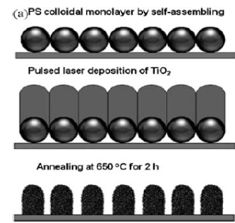
Figure 4. Schematic of the nanorod arrays fabricated on a PS monolayer by On Sphere gas phase deposition[1]
Shadowed oblique angle deposition (OAD)
This technique can be used to form one dimensional nanostructure arrays. The surface normal of a substrate in the deposition chamber is positioned at a large angle with respect to the oncoming vapour direction. This leads to a preferential growth of nanorods on the substrate in the direction of the deposition. The nanorods grow aligned but are tilted on the large substrate area. Periodic arrays are achieved by substrate patterning prior to deposition, due to the covering of the substrate with a PS monolayer. The patterned surface mounds are the nucleation sites for the OAD columns, since atomic shadowing of the deposition flux suppresses growth on the surrounding substrate. The close packed is due to the substrate being shadowed during deposition, due to the array of microspheres and then growing nanopillars. The nanopillars replicate the closed packed arrangement of the underlying microspheres.
Angle resolved nanosphere lithography
By varying the angle between the nanosphere masks and the beam of deposition new nanoarray structures can be made.
Nanogap: Nanogap structures were fabricated by first depositing material through a nanosphere mask mounted at a deposition angle of 0 ͦ and then depositing a second layer of material at or above an overlap threshold value of the deposition angle. The nanogap increases with increasing angle of deposition.
2021 Copyright OAT. All rights reserv
Nanooverlap:Nanooverlap structures were fabricated by first depositing material through a nanosphere mask mounted at a deposition angle of 0 ͦ and then depositing a second layer of material at or below an overlap threshold value of the deposition angle. The amount of nanoparticle overlap decreases with increasing angle of deposition. Nanooverlap structures allow predictable aspect ratio increases of double the original value [5].
Nanoparticle chains:This is fabricated by three consecutive depositions. The first deposition is done at 0 ͦ, the second deposition at deposition at 15 ͦ and -15 ͦ(tilted backwards), leading to high aspect ratio nanoparticles (Figure 5).
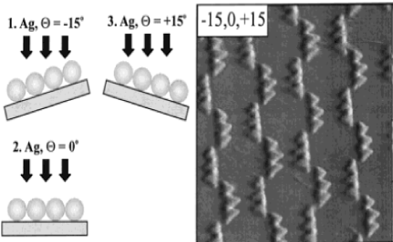
Figure 5. Nanoparticle chains made by Angle Resolved Nanosphere Lithography [5]
RIE and CF₄ Plasma Nanowell Structures
In order to create this structure a single monolayer of hexagonally close packed nanospheres is deposited on the substrate. The samples were placed in reactive ion etching (RIE) and exposed to CF₄ plasma. When plasma strikes the polystyrene nanospheres the hydrocarbons are fluorinated. This non volatile product is not etched away because the spheres stop the etching process. The plasma penetrates the holes in the sphere mask and radical products are etched away, leaving one with nanowell structures.
Functional multifaceted particle arrays
There has recently been a new strategy in the fabrication of arrayed colloidal particles each with nanopores in three fold or four fold symmetry. First a self organized double layer of PS microspheres was dipcasted and the spaces were filled with silica nanoparticles above the bottom layer and below the top layer. Partial RIE was then use to remove the top layer PS microspheres leaving behind an ordered monolayer of macropores in silica matrix. This was then used as a mask for further RIE processing. This left the PS microspheres having nanopores. The resulting nanopores are arranged in three fold or four fold symmetry depending on the stacking sequences of the PS microspheres. The threefold symmetry was created when the (111) plane of the PS microsphere was exposed to RIE etchant flow whereas the fourfold symmetry originated from the situation where the (100) plane was facing the etchant flow. The patterned array can be used for a variety of organic and inorganic materials such as metals for metal-polymer composites, DNA and proteins for biological applications, semiconducting and ceramic materials and other polymers and small chemicals for drug delivery can be incorporated via chemical and physical attachments (Figure 6).
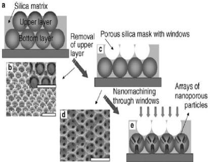
Figure 6. Nanolithography for the formation of multifaceted particle arrays[3]
In order to get micro particles with different shapes a separate method must take place. This process is called colloidal lithographic sculpting of microsphere arrays. This is done with PS or silica microspheres as was done above. Using ion etching the upper layer acts as a mask for the lower layers due to the shadowing effect. The resulting shapes were due to the crystal orientation relative to the etchant flow, the number of colloidal layers, and the size ratio of silica to PS microspheres, the etching angle in the RIE processes and the stacking sequence of the binary colloidal layers. The depth of the pores inside the PS particles can be controlled by the length of the RIE process.
Nanosphere lithography is an advanced process for the creation of nanostructures. This process makes large area periodic nanoarrays by applying colloidal suspensions onto a substrate. In order to have a substrate that has an ordered pattern of colloidal crystals one should use template directed colloidal self assembly which gives a long range order on a large area substrate.
Due to several different uses of nanoarrays one might want arrays of several different patterns. One can do this with several different patterning techniques to tailor the nanoarray product. Some of the resulting patterns are nanogaps, aligned one dimensional nanoarrays, an hncp arrangement etc. These different nanoarrays can be used in several different applications e.g. field emitters, light emitting diodes and anti reflection coat.
- Li L, Zhai T, Zeng H, Fang X, Bando Y, et al. (2011) Polystyrene sphere-assisted one-dimensional nanostructure arrays: synthesis and applications. Royal Society of Chemistry 1: 40-56.
- Oshima H (2013) Nanosphere Lithography for High-Density Nanopatterning in Vistas in Nanofabrication, Singapore. Stanford Publishing Pt. Ltd 1-26.
- Yang SM, Jang SG, Choi DG, Kim SHK (2006) Nanomachining by Colloidal Lithography. Small 2: 458-475.
- Barcelo SJ, Lam ST, Gibson GA, Sheng X, Henze D (2012) Nanosphere lithography based tehnique for fabrication of large area, well ordered metal particle arrays. Hewlett-Packard Development Company, Palo Alto.
- Haynes CL, Duyne V (2001) Nanosphere Lithography: A Versatile Nanofabrication Tool for Studies of Size-Dependent Nanoparticle Optics. Journal of Physical Chemistry 105: 5599-5611.