Preparation and gas barrier characteristics of polysilazane-derived silica thin films formed on PET by simultaneously applying ultraviolet-irradiation and heat-treatment have been investigated. Water-vapor-permeability of the thin film formed by UV irradiation at 100°C was 0.03 g/m2・day, indicating the good water-vapor resistance. The values of gas barrier characteristics depended on the substrate temperature at the time of photo irradiation. The TEM cross-sectional observation revealed that the gas barrier films were dense and uniform, and the reactive layer existed at the interface of the thin film and PET. The PET film with gas barrier thin film has good transparency in the region of visible light, flexibility as well as high gas barrier characteristics. This film-formation method is an effective way of forming a gas-barrier film at low temperature by using a film coating via an inorganic precursor solution.
polysilazane, photo-irradiation, gas barrier characteristics, PET film, flexible electronics
In recent times, as next-generation electronics products, devices featuring flexibility—such as flexible displays and electronic paper (characterized by their thinness, lightness, and bendability), flexible solar cells, and wearable devices—are gaining considerable attention [1-4]. Moreover, the so-called “flexible electronics” used to construct these products represent a field that is expected to grow rapidly from now onwards [5,6]. As essential elements required for creating flexible electronics, flexible substrates are indispensable component and make it possible to form various flexible devices. As for a flexible substrate, an organic-resin film with flexibility is generally used. A typical organic film, however, faces a major problem: its “gas-barrier” property (in regards to water vapor and oxygen) is poor, leading to oxidation of various device elements formed on the flexible substrate and degradation of device performance. As a result, it is necessary to develop a flexible substrate with an improved gas-barrier property. One means to improve the gas-barrier property of an organic film is to form a dense inorganic thin film on top of it. However, the low thermal resistance of an organic film means that it is a problem to form an inorganic film with good gas-barrier performance.
The most-common material used for organic films is polyethylene terephthalate (PET), and forming an inorganic thin film on a PET film improves the gas-barrier property of the PET. The thermal resistance of PET is limited to 100°C, so it has become mainstream to form metal oxide thin film like silicon-dioxide (SiO2) thin films on PET by using high-vacuum deposition apparatuses using methods like sputtering, vacuum deposition and atomic layer deposition (which restrain the heating temperature of the substrate) [7-12]. Unfortunately, the gas-barrier property of a SiO2 thin film is still insufficient, and using such complex high-vacuum equipment is one cause of increased costs. An alternative convenient method of forming an inorganic film is the application of an inorganic precursor solution. However, forming a dense inorganic thin film in this manner requires heating to several hundred degrees Celsius [13-17]. Applying this inorganic-precursor method in the case of organic films with low thermal resistance is thus difficult.
Recently, a method for forming a dense inorganic thin film on a PET film at low temperature—by excimer-light irradiation and ultraviolet (UV) irradiation of a polysilazane coating film—is being investigated [18-26], and an organic film (with an inorganic coating formed by that method) with a comparatively good gas-barrier property is being developed. Since this method uses a coating film applied by “printing” of an inorganic precursor solution, it is drawing considerable attention as a means of creating low-cost “printable electronics”. By irradiating a polysilazane coating film with UV light (by using a low-pressure mercury lamp) while heating the film, the authors have succeeded in developing an alicyclic polyimide film with high heat resistance and high transparency as well as a good gas-barrier property [27]. In the present study, a gas-barrier film on a PET film (with low heat resistance) was formed by using the same method using photo-irradiation and heat-treatment simultaneously, and the properties of the film were investigated .
Preparation of a silica thin film by photo irradiation
As a precursor for forming the film, a dibutyl-ether solution of polysilazane (NL-110, 20wt%; AZ Electronic Materials) was used. The dibutyl-ether (5wt%) solution of polysilazane was spin coated (at 1000 rpm for 60s) on a hydrophilized PET film (A7300; thickness: 100μm, Toyobo Ltd.) subjected to corona-discharge treatment. The surface of the spin-coated film was irradiated with light from a low-pressure mercury lamp in air. The photo-irradiation intensity was 12 mW/cm2 for 20 minutes. And the substrate was heated to temperature of 80°C or 100°C during the photo irradiation. The thin inorganic film was formed on both sides of the PET film. Samples composed of either single or double coatings of polysilazane film were prepared. For comparison, samples subjected to thermal treatment (80°C or 100°C, 60 min.) only were also prepared.
Change of the molecular structure of the thin film was observed by means of infrared absorption spectra (FTIR-8400S, Shimadu Co.). Absorption and reflection of the film were measured by means of ultraviolet and visible absorption spectroscopy (UV-2450, Shimadu Co.). As for reflectance, the rear surface of the PET film was subjected to blackening treatment, and a 5° specular reflectance was measured. The cross-sectional structure of the thin film was observed by transmission electron microscope (TEM: H-9000NAR, Hitachi Ltd.). The TEM specimens were prepared by focused-ion beam (FIB) processing. And cross-sectional observation and elemental analysis were performed by scanning transmission electron microscope (STEM:HITACHI SU8230, Hitachi Ltd.).
X-ray photoelectron spectroscopy (XPS: Quantera SXM, PHI Co.) was used for elemental analysis of the upper surface of the thin film during sputtering. The gas-barrier property was measured in terms of water-vapor permeability (at 40°C and 90% RH) by a permeation testing system (MOCON PERMATRAN-W). As for water-vapor permeability of more than 1 g/m°・day, it was measured by the dish method. Water-vapor permeability was measured under the following conditions: temperatures of 40°C, 50°C, and 55°C and humidity of 90%RH. Adhesion strength between the thin film and the PET film was estimated by tape-peel test in accordance with Japan Industrial Standards, JIS K5600-5-6.
Surface condition and property of gas-barrier film
In consideration of the heat-resistance temperature of PET, the gas-barrier film was fabricated by photo irradiation at a temperature of 100°C. Photographs showing the surface condition of the PET film with the gas barrier formed on its surface are shown in Figures 1(a) and (b). As clear from the former photograph, the transparency of the fabricated film is very high. As clear from the latter photograph, its flexibility, and thereby bendability, is also high, so no cracks are generated in the film. It is clear from the laser-microscope image of the film shown in Figure 1(c) that a uniform thin film is formed on the substrate. As for the adhesive strength of the thin film with the PET-film substrate, strong adhesion of 100/100 (remaining number of sheets/number of cuts) was revealed by a JIS-standard tape-peel test.

Figure 1. Appearance and surface photographs of gas barrier film (2-coated film) prepared by photo irradiation
Variation of visible-UV absorption spectra and infrared absorption spectra due to photo irradiation of polysilazane coating film
Variation of visible and UV absorption spectra due to ultraviolet irradiation of the polysilazane coating film formed on a quartz substrate is shown in Figure 2. The just-formed film (i.e., no UV irradiation) shows broad absorption around a wavelength of 320 nm and weaker absorption in the wavelength range of 600 to 800 nm. Moreover, it shows strong absorption in the UV region below 260 nm. When the film was irradiated by UV light, while the temperatures rises during the irradiation, these absorptions are greatly reduced in a manner that absorption is no longer shown across the range from UV wavelengths to visible wavelengths.
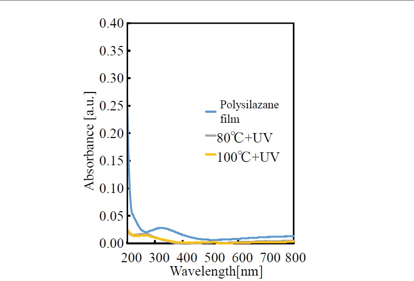
Figure 2.Spectral changes of absorption spectra of polysilazane thin film photo-irradiated at 80°C, 100°C
Variation in the IR-absorption spectra of thin film fabricated under the same conditions as stated above is shown in Figure 3. The just-formed film shows absorption due to NH (around 3300 cm-1), SiH (around 2200 cm-1), and SiN (around 800 cm-1), and it is presumed that the film has a structure composed of Si-N bonds. These absorptions are decreased as photo-irradiation temperature increases from room temperature, to 80°C, and finally to 100°C. At the same time, absorption due to siloxane bonds (-O-Si-O-) around 1100 cm-1 gets more pronounced. However, even in the case of photo-irradiation at 100°C, slight absorption due to SiN is shown around 800 cm-1, and it is presumed that the polysilazane film is not completely transformed to SiO2. The film heat-treated at 100°C ( no UV-irradiation) shows strong absorption peak due to polysilazane.
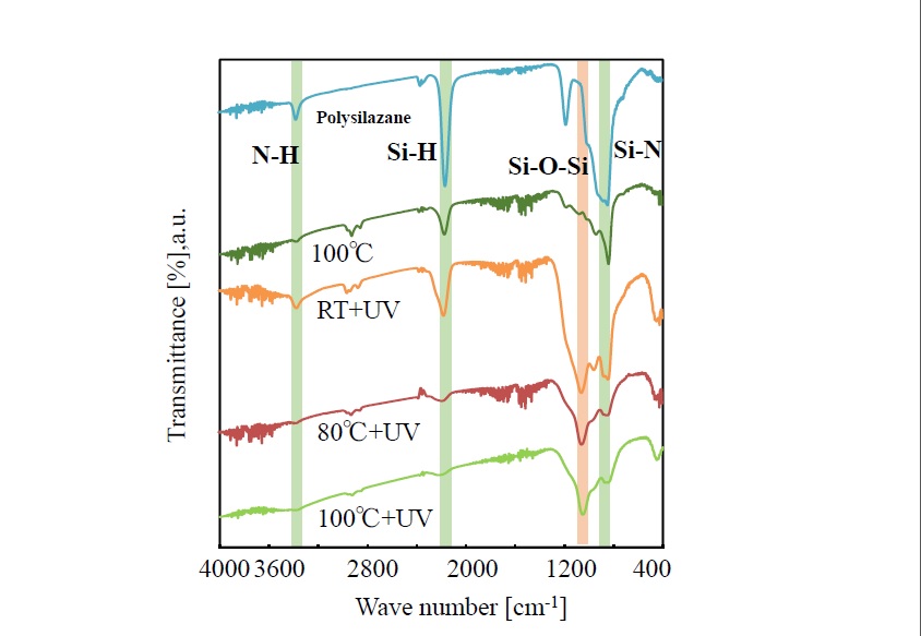
Figure 3.Spectral changes of infrared spectra of photo-irradiated films
Transmittance and reflectance spectra of the polysilazane film formed on the PET film
Transmittance and reflectance spectra of the polysilazane film formed on the PET film are shown in Figure 4. The PET film shows transmittance of about 90% (i.e., almost no absorption) in the wavelength range from 380 to 800 nm. It is clear from the figure that when the polysilazane film is formed on the PET film, as the photo-irradiation temperature is increased (from RT to 80°C and then from 80°C to 100°C), transmittance at wavelengths below about 500 nm decreases, but that above about 500 nm increases. On the other hand, although reflectance of 7.2% to 7.7% is shown in the wavelength region of 350 to 380 nm, and above 500 nm, it drops to 3.5% to 3.7%. The finding that the transmittance curves fall below that of the PET film itself below about 500 nm and rise above it above about 500 nm is presumed to be connected to the fact that the reflectance of the thin-film-coated PET film increases rapidly below about 500 nm but decreases above 500 nm. In other words, as the reflectance of the film surface is increased, the transmittance of the film is decreased. It is thus conceivable that the transmittance is increased in correspondence with the lowering of the surface reflectance. It is also conceivable that the variation of surface reflectance is due to a SiO2 thin film (with low refractive index) being formed on the PET film.
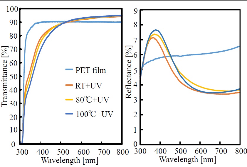
Figure 4. Transmittance and reflectance spectra of photo-irradiated films
Cross-sectional observation of the film by TEM
Cross-sectional TEM images of thin films irradiated at 100°C with a single-polysilazane-film coating [image (a)] and a double-polysilazane-film coating [image (b)] are shown in Figure 5. The thicknesses of the single- and double-layer-coated films were observed as 109 and 222 nm, respectively. In other words, laminating the coatings in this way doubled the thickness of the coating film. Although the surface and cross-section of the films were uniform, a reactive layer was observed at the interface with the PET film. It is presumed that this reactive layer is a surface-modification layer formed by the corona-discharge treatment applied to improve the wettability of the polysilazane solution on the surface of the PET film.
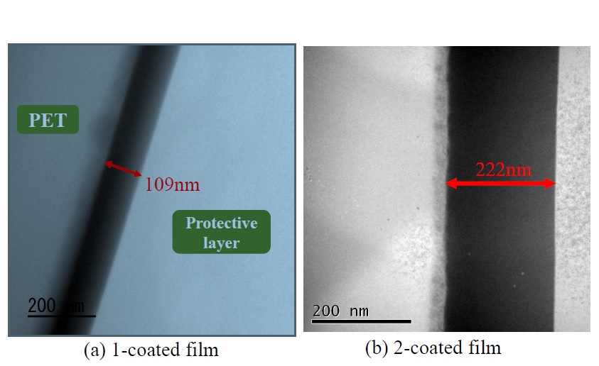
Figure 5. Cross-sectional TEM photographs of 1-coated and 2-coated films
A cross-sectional STEM image of the double-coated film and results of EDX analysis (silicon, carbon, and oxygen) of the film are shown in Figure 6. In the STEM image, the condition of the reactive layer at the interface of the SiO2 film and the PET can be clearly seen. Moreover, a clear laminate interface between the first and second polysilazane coating films cannot be seen.
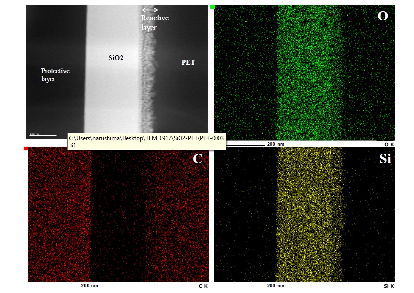
Figure 6.Cross-sectional SEM photographs of the 2-coated films and EDX analysis
As shown by the results of EDX analysis, silicon exists not only in the SiO2 layer derived from polysilazane but also in the interfacial-reaction layer. On the other hand, although a dense distribution of carbon can be seen on the PET substrate, carbon is also distributed in the interfacial-reaction layer. This observation suggests that the interfacial-reaction layer exists in a state in which SiO2 (derived from polysilazane) and carbon (derived from PET) are mixed. It is presumed that the polysilazane solution penetrates as far as the surface modification layer (due to the corona-discharge treatment for hydrophilization) and, under this condition, it is transformed to SiO2.
XPS spectra
Depth profiles (Si2p, O1s, N1s, and C1s) obtained by XPS elemental analysis of the single-coated film are shown in Figure 7. The Si/O ratio in the SiO2 film (i.e., 1.7 to 1.8) is slightly lower than the stoichiometric ratio (namely, 2.0). It is conceivable that the composition of the SiO2 film is given by SiOx(X<2). In this region, carbon is not observed in the profiles. Moreover, nitrogen at concentration of 2 to 3 at.% can be observed across the entire thin film. In the interfacial-reaction layer between the SiO2 film and PET substrate, silicon, oxygen, carbon, and nitrogen are observed. Although the concentrations of silicon and oxygen in the depth direction of the film gradually decrease, that of carbon increases rapidly as the PET-film substrate is approached. Nitrogen concentration in the interfacial region with PET increases slightly (to 4 to 6 at.%) compared to that in the SiO2film. It is conceivable that this increase is due to nitrogen generated by penetration of the polysilazane solution into the interfacial-reaction layer. It is thus suggested that the interfacial-reaction layer exists in a state in which SiOx components and organic-polymer components are mixed.
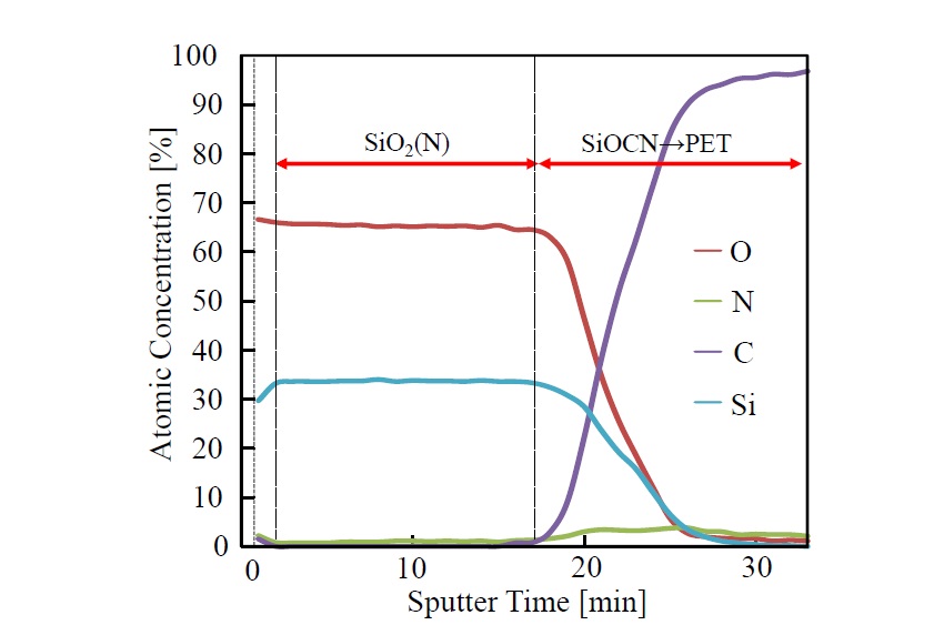
Figure 7.XPS depth profile of elemental analysis of the 1-coated film photo-irradiated at 100°C
The manner in which XPS peaks (for Si2p, O1s, N1s, and C1s) in the depth direction change is shown in Figures 8 and 9. It is clear that the Si2p peak (shown near 103.8 eV) broadens with increasing sputtering time, and the peaks corresponding to SiON and SiOx become combined. The divergence from the compositional ratio of SiO2 in the depth direction increases. In the same manner as the Si2p peak, the O1s peak broadens in the depth direction as the peak intensity weakens. The N1s peak can be seen at the outermost surface, but it weakens after sputtering for one minute. After that, as sputtering time increases, the peak gradually gets stronger. Although the C1s peak shows a similar trend, it cannot be seen from sputtering times of one to 19 minutes. After 19 minutes, however, it rises rapidly. The weak intensities of the N1s and C1s peaks observed at the outermost surface are presumed to be due to contamination by impurities on the surface.
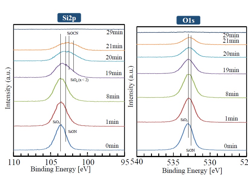
Figure 8. XPS peak depth profile of each element (Si2P, O1S)
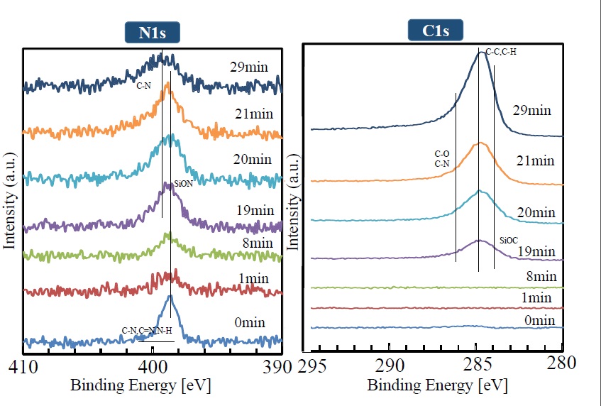
Figure 9.. XPS peak depth profile of each element (N1S, C1S)
Gas-barrier property
Water-vapor transmission rates of the UV-irradiated single-coating films at r.t., 80°C ,100°C and the UV-irradiated double-coating film at 100°C in comparison with that of the single-coating films heat treated at 80°C, 100°C are shown in Figure 10. Although the water-vapor transmission rate of the PET substrate on its own is 6.8 g/m2・day, and when the polysilazane film was formed by heat drying at 80°C and 100°C, that value decreased slightly (to 6.5 and 5.7 g/m2・day, respectively), the value hardly changed from that of the PET itself. On the other hand, while the substrate temperature increases during UV-irradiation film processing, the value is decreased significantly. Although the value of the film UV-irradiated at room temperature without heating the substrate (i.e., 6.6 g/m2・day) is not significantly decreased compared to the value of the PET film itself (6.8 g/m2・day), it decreases significantly on heat treating the substrate at 80°C and 100°C (to 1.9 g/m2・day and 1.2 g/m2・day, respectively). Moreover, when a double-layer coating film is formed by UV-treatment at 100°C, water-vapor transmission rate is reduced to 0.03 g/m2・day; in other words, a good gas-barrier property is attained. These results demonstrate that film thickness has a significant influence on the gas-barrier property.
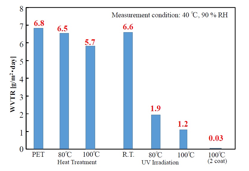
Figure 10.Water vapor transmission rates of photo-irradiated films
Temperature dependence of water-vapor transmission rate of the double-coating film by UV irradiation at 100°C was measured. A natural-log plot of measured water-vapor transmission rate under certain conditions (temperatures of 40°C, 50°C, and 55°C and relative humidity of 90%) against the reciprocal plot of temperature is shown in Figure 11. Three measurement points (i.e., temperature/water-vapor transmission rate: 40°C; 0.03 g/m2・day, 50°C; 0.54 g/m2・day, and 55°C; 1.30 g/m2・day) are plotted. The activation energy of water-vapor transmission (obtained from the slope of the straight line by using the Arrhenius equation) is 219 kJ/mol. Moreover, water-vapor transmission at room temperature (25°C)—determined by extrapolating the line—is given as an extremely low value (i.e., 4.5 × 10⁻⁴ g/m2・day).
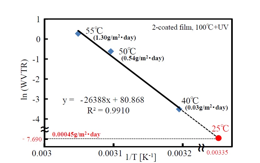
Figure 11. Temperature dependency of WVTR of the 2-coated film
Polysilazane shows strong absorption in the UV region below 260 nm; in particular, it absorbs light with wavelengths of 254 and 185 nm (i.e., UV-luminescence wavelengths from a low-pressure mercury lamp). UV light with these wavelengths corresponds to energies of 113 kcal/mol (254 nm) and 155 kcal/mol (185 nm). Meanwhile, the binding energies of the Si-N, Si-H, and N-H bonds of polysilazane are 105, 71, and 92 kcal/mol, respectively. In other words, the energy of the UV beam is bigger than these binding energies and thus sufficient to break the bonds. The broken bonds are instantaneously switched to oxidized SiO2 by reactive oxygen species such as singlet oxygen [O(1D)] and active oxygen like ozone (O3) generated by UV irradiation and oxygen in the atmosphere. It is conceivable that at that time, diffusion of the active species in the film is increased when the temperature is increased during UV irradiation, and oxidation of silicon is further promoted. It is also conceivable that the phenomenon by which the absorption in the visible and UV regions is decreased by photo-irradiation (as shown in the absorption spectra in Figure 2) is due to the transformation of polysilazane to SiO2. Absorption in the UV region is significantly decreased, and a clear inorganic thin film that shows no absorption in the visible region is obtained.
As for the IR spectra, decreasing absorption of N-H, Si-H, and Si-N bonds derived from polysilazane as the temperature during photo-irradiation rises and the broadening peak corresponding to the Si-O-Si bond derived from SiO2 also confirm generation of SiO2. However, as for the film photo-irradiated at 100°C, absorption due to Si-N bonds remains in the IR-absorption spectra. It is thus conceivable that although SiO2 is present as the main component, chemical species with bonds such as SiON are also present. And according to the results of XPS analysis, the SiO2 layer has a SiOx(x<2) composition slightly lower than the stoichiometric composition, and nitrogen concentration in the film was predicted to be 2 to 3 at %.
From this XPS results too, it is conceivable that the irradiated film is not completely converted to SiO2. The XPS analysis in the depth direction of the film reveals a clear trend: the proportions of SiON and SiOx(x<2) gradually increase going in the depth direction even though SiO2 is the main component in the outermost surface layer. This trend indicates that oxidation of the film progresses in the depth direction of the film from the outermost surface. It is conceivable that it indicates that light is irradiated from the outermost surface and diffusion of the active oxygen species into the film progresses from the outermost surface. The results of the cross-sectional TEM and STEM observations of the thin film indicate that the film is in a fine state and integrated with the laminated coating; that is, an interface between them does not exist. Moreover, the double-coating film is about twice as thick as the single-coating film, and it is expected that a fine and integrated film is formed by laminate coating and the film contributes to improving the gas-barrier property.
Elemental analysis by XPS and STEM revealed carbon due to the organic-resin component of PET and the SiO2 component from the interfacial-reaction layer between the thin film and PET, and it is supposed that polysilazane in this region penetrates the surface of the PET. This penetration is manifested as an “anchor effect,” which possibly contributes to improving the adhesive force at the PET surface of the thin film.
The gas-barrier property depends on the formation conditions and thickness of the thin film. It is possible that the gas-barrier property is greatly enhanced by formation of the lamination layers when the substrate temperature is raised during photo-irradiation. The double-coated thin film photo-irradiated at 100°C showed a water-vapor transmission rate (0.03 g/m2・day) near the measurement limit of the measurement apparatus (0.02 g/m2・day). The logarithmic value of the gas-barrier property when the temperature of the water-vapor-permeability measurements of the double-coated thin film is changed from 40°C, to 50°C, and then to 55°C shows a linear relation with the reciprocal of temperature in accordance with the Arrhenius equation. When the value of water-vapor permeability at 25°C was calculated from the Arrhenius plot, an extremely low value (4.5 × 10⁻⁴ g/m2・day) was obtained, and that low permeability value indicates the good gas-barrier property of the film.
After heat treatment at 80°C and 100°C without photo-irradiation, the gas-barrier properties hardly change compared to the value of PET, suggesting that the gas-barrier property is improved by refinement of the thin film formed by photo-irradiation. After heat treating the thin film at 80°C and 100°C, strong absorption due to polysilazane in IR-absorption spectra was observed (Figure 3), implying that the transformation from polysilazane to SiO2 is completely insufficient. Moreover, the gas-barrier property of the thin film photo-irradiated at room temperature shows no significant difference from that of the PET film. Accordingly, it is understood that the temperature during photo-irradiation is a key factor in forming a dense film with a good gas-barrier property. The thin film photo-irradiated at room temperature also showed infrared absorption due to polysilazane, so it is supposed that the chemical structure and thickness of the film, as well as its density, is a key factor in improving the gas-barrier property.
The effect of UV irradiation of a polysilazane coating formed on a PET film and the influence of the UV irradiation on the gas-barrier property of the film were investigated. Water-vapor-permeability of the thin film formed by UV irradiation at 100°C, namely, 0.03 g/m2.day (at 40°C/90%RH) demonstrated the good water-vapor resistance of the film. The temperature of photo-irradiation has a significant effect on the gas-barrier property of the film, which was considerably enhanced above 80°C. Although the main component of the thin film is SiOx(X<2), it was inferred that the film also includes a SiON component due to some remaining nitrogen derived from the polysilazane. The thin film has a dense structure, and the thickness of the double-coating film was 222 nm. Cross-sectional observation by TEM showed that a reactive layer exists at the interface of the thin film and PET film. According to the results of investigation of temperature variation of water-vapor permeability, it is inferred that the developed film has an excellent gas-barrier property, namely, 4.5 × 10⁻⁴ g/m2・day at 25°C. This film-formation method is an effective way of forming a gas-barrier film at low temperature by using a film coating via an inorganic precursor solution.
This work was supported by JSPS KAKENHI Grant Number 26420711.
- White MS, Kaitenbrunner M, G Istrokowacki ED, Gutnichenko K, Kettlgruber G, et al. (2013) Ultrathin highly flexible and stretchable PLEDs. Nature Photonics 7: 811-816
- Sekitani T, Someya T (2011) Human-friendly organic integrated circuit. Materials Today 14: 398-407
- Sekitani T, Zschieschang U, Klauk H, Someya T (2010) Flexible organic transistor and circuits with extreme bending stability. Nature Materials 9: 1015-1022
- Nomura K, Ohta H, Kamiya T, Hirano M, Hosono H (2004) Room-temperature fabrication of transparent flexible thin-film transistors using amorphous oxide semiconductors. Nature 432: 488-492
- Wong WS, Salleo A (2009) Flexible Electronics: Materials and Applications. Springer New York
- Sekitani T, Someya T (2010) Stretchable Large-area Organic Electronics. Advanced Materials 22: 2228-2246
- Carcia PF, Mclean RS, Groner MD,2021 Copyright OAT. All rights reservfusion ultrabarriers on polymer substrates using Al2O3 atomic layer deposition and SiN plasma-enhanced chemical vapor deposition. Journal of Applied Physics 106: 023533
- Yagi Y, Akashi K (2007) Passivation films on organic film substrates designed for organic electroluminescence device. Journal of Vacuum Society of Japan 50: 735
- Hanada T, Negishi T, Shiroishi I, Shiro T (2010) Plastic substrate with gas barrierlayer and transparent conductive oxide thin film for flexible displays. Thin Solid Films 518: 3089
- Hata T, Nakayama H (2008) An organic catalytic CVD: Principle, apparatus and applications. Thin Solid Films 516: 558
- Carcia PF, MacLean RS, Reilly MH, Groner MD, George SM (2006) Catalyst of Al2O3 gas diffusion barriers grown by atomic layer deposition on polymer. Applied Physics Letters 89: 031915
- Dameron AA, Davidson SD, Burton BB, Carcia PF, MacLean RS, et al. (2008) Gas diffusion barriers on polymer using multi layers fabricated by Al2O3 and rapid SiO2 atomic layer deposition. Journal of Physical Chemistry C 112: 4573-4580
- Brinker CJ, Schere GW (1990) Sol-Gel Science. Academic Press Boston
- Seyferth D, Wiseman GH (1984) High-yield synthesis of Si3N4/SiC ceramic materials by pyrolysis of a novel polyorganosilazane. Journal of American Ceramic Society 37: 132
- Kamiya K, Oka AI, Nasu H, Hashimoto T (2000) Comparative study of structure of silica gels from different sources. Journal of Sol-Gel Science & Technology: 495-499
- Iwamoto Y, Sato K, Kato T, Inada T, Kub Y (2005) A hydrogen-perselective amorphous silica membrane derived from polysilazane. Journal of European Ceramic Society 25: 257
- Funayama O, Tshiro Y, Kamo A, Okumura M, Isoda T (1994) Conversion mechanism of perhydropolysilazane into silicon nitride-base ceramics. Journal of Material Science 29: 4883-4888
- Ohishi T (2003) Gas barrier characteristics of a polysilazane film formed on an ITO-coated PET substrate. J Non-Cryst. Solids 330: 248
- Naganuma Y, Tanaka S, Kato C, Shindo T (2004) Formation of silica coating from perhydropolysilazane using vacuum ultraviolet excimer lamp. J Ceram Soc Japan 112: 599
- Prager L, Dierdorf D, Liebe L, Naumov S, Stojanovic S, et al. (2007) Conversion of perhyropolysilazane into SiOx network triggered by vacuum ultraviolet irradiation. Chem. Eur. J 13: 8522
- Kobayashi Y, Yokota H, Fuchita Y, Takahashi A, Sugawara A (2013) Characterization of gas barrier silica coating prepared from perhydropolysilazane films by vacuum ultraviolet irradiation. J Ceram Soc Japan 121: 215
- Morlier A, Cros S, Garandet JP, Alberola N (2012) Thin gas-barrier silica layers from perhydropolisilazane obtained through low temperature curing: A comparative study. Thin Solid Films 524: 62-66
- Naganuma Y, Horiuchi T, Kato C, Tanaka S (2013) Low-temperature synthesis of silica coating on a poly(ethylene terephthalate) film from perhydropolysilazane using vacuum ultraviolet light irradiation. Surface & Coatings Technology 225: 40-46
- Morlier A, Cros A, Garandet JP, Alberola N (2013) Gas barrier properties of solution processed composite multilayer structures for organic solar cells encapsulation 115: 93-99
- Morlier A, Cros S, Garandet JP, Alberola N (2014) Structural properties of ultraviolet cured polysilazane gas barrier layers on polymer substrates. Thin Solid Films 550: 85-89
- Blankenburg L, Schrodner M (2015) Perhydropolysilazane derived silica for flexible transparent barrier foils using a reel-to-reel wet coating technique: Single- and multilayer structures. Surface & Coatings Technology 275: 193-206
- Ohishi T, Sone S, Yanagida K (2014) Preparation and gas barrier characteristics of polysilazane-derived silica thin films using ultraviolet irradiation. Materials Sciences and Applications 5: 105-111