We report experimental results for C60-Si deposition by simultaneous thermal vaporization of fullerene source and chemical vapor deposition from silane source. The samples were characterized by Scanning Electron Microscopy, Energy-dispersive X-ray spectroscopy, Micro-Raman spectroscopy, Wide-angle X-ray scattering, X-ray photoelectron spectroscopy and its thermal stability was studied, discussed and compared with pure C60 deposited by the same method. A crystalline material was obtained and results suggest that a polymerization of fullerenes bridged by silicon atoms was achieved.
Many works have been published about fullerenes and in particular about C60 or buckyminsterfullerene, the most stable of fullerenes. Its properties are of great value in a diversity of applications like organic solar cells, hydrogen gas storage, metals strengthening/hardening, optical limiters, solid sensors, drug carriers, etc [1-8]. The fabrication of novel nanostructured materials from fullerenes is promising for several of these applications. However weak van der Waals bond between fullerenes is a serious limitation for some applications and polymerization has been a vastly studied solution. A variety of fullerene polymers were reported, using photopolymerization, pressure-induced polymerization, charge-transfer polymerization mediated by metals, electron beam-induced and plasma-induced polymerization as some strategies to prepare the so-called all-carbon polyfullerenes [9-15]. In particular, using Group IV elements in order to bind fullerene molecules has been investigated and both theoretical and experimental works about fullerenes molecules bonded by silicon bridges have been published by Masenelli et al. and Fujiwara et al. [16-19], which motivates the possibility to construct a polymerized fullerene-silicon material.
We report experimental results for deposition of C60-Si material by simultaneous thermal vaporization of fullerene source and chemical vapor deposition from silane source. The materials produced were characterized by Scanning Electron Microscopy, (SEM), Energy-dispersive X-ray spectroscopy (EDS), Micro-Raman spectroscopy, Wide-angle X-ray scattering (WAXS), X-ray photoelectron spectroscopy (XPS) and their thermal stability was also studied.
Fullerene and Si were deposited on Ge (100) and Si (100) wafers in a vacuum chamber. Fullerene source was pristine C60 powder (99.9% C60) evaporated at 550º C and silane (SiH4) was introduced in the chamber and dissociated on a tungsten hot filament in order to incorporate silicon atoms to the C60 lattice. Fullerene source was degassed in situ at 300º C and 5.10-7 mbar for several hours in order to release the oxygen that could be trapped in it. The deposition process was carried at 5.10-5 mbar with both evaporated fullerene and dissociated silane mixing in the chamber. The substrate was polarized at -30 V during the process. Substrates were cleaned by an acetone ultrasonic bath. For the sake of comparison, pure fullerene and pure silicon were separately deposited in the same conditions and by the methods used for the mixed samples. Also, in some samples pure fullerene and C60-Si were simultaneously deposited in different zones of the substrate, in order to compare the thermal stability of each material under the same conditions.
Both pure fullerene and fullerene-silicon samples were analyzed by Scanning electron microscopy (SEM), Energy-dispersive X-ray spectroscopy (EDS), Micro-Raman spectroscopy, Wide-angle X-ray scattering (WAXS) and X-ray photoelectron spectroscopy (XPS). Microscopy was carried on by a SEM Carl Zeiss NTS SUPRA 40. Raman spectra were recorded using a LabRAM HR Raman system (Horiba Jobin Yvon), equipped with a confocal microscope and a charge coupled device detector (CCD). A 100X objective lens was used, generating a 1.5 μm spot. An 1800 g/mm grating and 100 μm hole results in a 2 cm−1 spectral resolution. The 514 nm line of an Ar+ laser was used as excitation source. The laser power density over the sample was between 0.4 W.mm−2 and 4 W.mm−2. WAXS experiments were performed at INIFTA facilities using a XEUSS 1.0 equipment from XENOCS with a Kα-Cu radiation micro-source. A PILATUS-100K detector was used with 13 cm sample detector distance. One-dimensional curves were obtained by integration of the 2D data using the Foxtrot program. The scattering intensity distributions as a function of the scattering angle (2θ) were obtained in the 2θ range between 3º and 39°. The samples were placed in a motorized sample holder suitable for grazing incidence measurements at room temperature. XPS experiments were made using a Multitécnica Specs equipped with a dual Ag/Al monochromatic X-ray source and a PHOIBOS 150 hemispheric analyzer in fixed analyzer transmission mode (FAT). The spectra were obtained with 30 eV energy and an Al monochromatic anode at 300 W. The measurements were made on a 2 mm2 area over the sample and at different depths, removing material by sputtering. For the data analysis, the spectra were fitted by Gaussian/Lorentzian convolution functions with a previous optimization of the background parameters. The background was modeled by a Shirley background function.
Some deposited samples were annealed in vacuum (5.10-7 mbar) at 600º C after deposition in order to study the material thermal stability.
SEM images for pure fullerene and C60-Si samples are shown in Figure 1. In the later, hexagonal structures of a few μm are clearly observed, a major morphologic difference with pure C60 samples. EDS measurements over several points at different crystals on C60-Si samples grown on Ge (100) substrates, mainly detected both C and Si presence at an atomic ratio less than 2% Si respect to C. Also, a weak signal of oxygen was measured, which could have been absorbed after deposition when exposed to air. Germanium corresponding to the substrate was also observed.
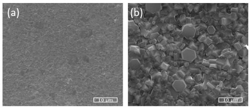
Figure 1. SEM images for pure deposited C60 (a) and deposited C60-Si (b).
Raman spectra from pristine, deposited fullerene and from C60-Si samples are shown in Figure 2. If a power density above 4 W/mm2 is used a clear change in the spectra is observed. The spectra show no significant differences between the samples. The breathing frequencies of pristine fullerene were observed in both deposited C60 and C60-Si samples, indicating that fullerenes were not broken during deposition. Si-Si signal was not observed, suggesting that there was not Si segregation. The spectra for pure silicon samples show the characteristic bands of amorphous silicon [20].
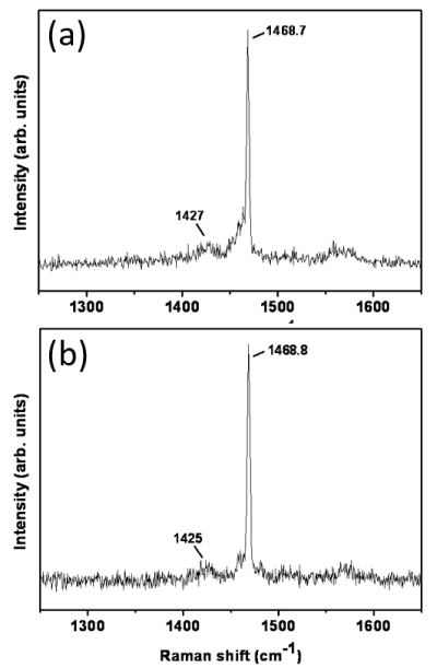
Figure 2. Raman spectra for pure C60 (a) and C60-Si (b) deposited samples.
WAXS results are shown in Figure 3. Peaks corresponding to cubic and hexagonal (marked by arrows) fullerene structures are observed in both deposited C60 and C60-Si samples [21]. Broader peaks than in the case of pristine fullerene (our source material) could indicate smaller grain sizes. Peak positions for the cubic symmetry are the same for all samples and this implies that silicon atoms among fullerenes are not significantly changing the lattice parameters nor the distance between fullerenes. WAXS pattern’s peaks after 600º C in vacuum annealing become a little thinner, but both cubic and hexagonal phases are still present.
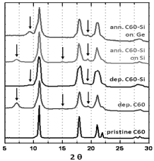
Figure 3. WAXS patterns from pristine C60, deposited C60 and C60-Si on Si(100) wafer and C60-Si samples deposited on Si(100) and Ge(100) wafers and annealed to 600º C after deposition.
As cubic phase was the predominant one, numerical calculations were made using the semiempirical many-body Tersoff potentials, which had been used and achieved a good description of carbon fullerenes, including several polymeric phases [14,22]. A zincblende C60-Si structure was found to be stable.
Results for XPS measurements for annealed C60-Si samples are shown in Figure 4. The peaks can be assigned to Si2p, Si2s, C1s and O1s. The peaks position and width shown in Fig 4. lightly change at different depths. An atom proportion of 53.4% carbon, 27.2% silicon and 19.4% oxygen was found (after 60 seconds of argon sputtering at 1000 V), which ensures an enough quantity of silicon in order to conform a zincblende structure as proposed in the simulation results.
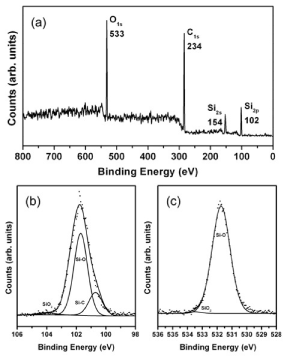
Figure 4. XPS measurement for C60-Si deposited sample. (a) survey and fitting for Si2p (b) and O1s (c) signals
In Figure 4 (b) and (c) the analysis for Si2p and O1s XPS signals is shown. The envelop of each Si2p contribution was the result of 2p 3/2 and 2p 1/2 orbitals summation where the doublet separations energy and the branching ratio were fixed in 0.6 eV and 0.5 eV respectively. From the Si2p signal analysis, a proportion of 21.7% Si-C, 1.6% SiO2 and 76.7% Si-O was calculated. For O1s signal, mostly Si-O was found, which could be attributed to some species like CSiOn (n<3) [23], and around 1% of SiO2. It is hard to fit correctly for C1s signal, as C-C bonds are indistinguishable from C-Si ones. But the peak is consistent with a mixture of signals from C-Si, C-C (sp3 carbons) and C=C (sp2 carbons) bonds. By analyzing O1s and C1s results, it can be ensured that a negligible amount of C=O and C-O bonds are present in the sample [24-28].
The thermal stability is the most outstanding result. While deposited C60 samples are completely wiped out when annealed in vacuum at 600º C, leaving the substrate totally clean, C60-Si samples morphology and Raman spectra are unchanged. Even for the samples where pure fullerene and C60-Si were simultaneously deposited in different zones of the substrate, the C60 was completely removed while the mixed material remained unaltered. This result implies that covalent bonds were formed between fullerenes.
It was observed that crystalline structures are formed when C60 and silicon are simultaneously deposited by the described method. This is clearly suggested by the shapes observed by SEM and confirmed by WAXS. Looking at the diffractograms is possible to affirm that cubic fcc and hexagonal structures are present in the sample, the former in agreement with our simulation results. While both could be assigned to a pure C60 material, the presence of silicon was confirmed by EDS and XPS also no evidence of segregation was found. Moreover, XPS analysis evidenced a considerable proportion (27.1%) of silicon atoms bonded to carbon atoms, but measuring over individual crystals by EDS a relation lesser than 2% was found between silicon and carbon atoms. Even more significant, the samples show no perceptible alterations after an annealing at 600º C, a temperature at which pure C60 samples deposited by the same method were completely cleaned. This suggests that covalent bonds were formed between fullerenes when C60 deposition is carried simultaneously with silicon deposition. Moreover, calculations employing the semiempirical many-body Tersoff potential found a zincblende structure to be stable and such configuration is in concordance with most of our experimental results.
WAXS experiments at INIFTA were performed thanks to project “Nanopymes” (EuropeAid/132184/D/SUP/AR-Contract31-896).
- Ulloa E (2013) Fullerenes and their Applications in Science and Technology, 4138296, EEE-5425, Introduction to Nanotechnology, Spring.
- Goodarzi S, Ros TD, Conde J, Sefat, F, Mozafari M (2017). Fullerene: biomedical engineers get to revisit an old friend. Mater Today 20: 460.
- Klupp G, Margadonna S, Prassides K (2001) Encyclopedia of Materials: Science and Technology 3379.
- Ganesamoorthy R, Sathiyan G, Sakthivel P (2017) Fullerene based acceptors for efficient bulk heterojunction organic solar cell applications Mat Sol C 161: 102.
- Coro J, Suárez M, Silva LSR, Eguiluz KIB, Salazar-Banda GR (2016) Fullerene applications in fuel cells: A review. Int J Hydrogen Energ 41: 17944
- EL-Barbary AA (2016) Hydrogenation mechanism of small fullerene cages. Int J Hydrogen Energ 41: 375.
- Gaboardi M, Amadé NS, Aramini M, Milanese C, Magnani G (2017) Carbon 120: 77
- Dong Y, Saini D, Echegoyen LA, Podila R (2016) Passive optical switches based on endohedral fullerenes. Optical Materials 53: 14.
2021 Copyright OAT. All rights reserv
- Melinon P, Masenelli B (2012) From Small Fullerenes to Superlattices: Science and Applications. CRC Press.
- Tanaka H, Osawa S, Onoe J, Takeuchi K (1999) Formation Process of Si-Coated C60. J. Phys. Chem 103: 5939.
- Tournus F, Masenelli B, Melinon P, Blasé X, Perez A (2002) Bridging C60 by silicon: Towards non-Van der Waals C60-based materials. Phys. Rev. B 65: 165417
- Reinke P, Oelhafen P, Christiansen S (2002) Three-dimensional structures formed with C 60 and amorphous silicon--a feasibility study on the formation of a composite material. Surface Science 507-510: 630-635.
- Berber S, Osawa E, Tománek D (2014) Rigid crystalline phases of polymerized fullerenes. Phys. Rev. B 70: 085417.
- Burgos E, Halac E, Weht R, Bonadeo H, Artacho E, et al. (2000) New superhard phases for three-dimensional C60-based fullerites Phys Rev Lett 85: 2328-2331. [Crossref]
- Giacalone F, Martín N (2006) Fullerene polymers: synthesis and properties. Chem Rev 106: 5136-5190. [Crossref]
- Masenelli B, Tournus F, Mélinon P, Pérez A, Blasé X (2002) Ab initio study of C60C60–silicon clusters J. Chem. Phys 117: 10627.
- Masenelli B, Tournus F, Mélinon P, Blasé X, Perez A (2004) Nanostructured films from (C60)nSim clusters. Appl. Surf. Sci 226: 226.
- Masenelli B, Tournus F, Melinon P, Blasé X, Perez A (2003) Surf. Sci 532-535: 875.
- Fujiwara K, Komatsu K (2002) Mechanochemical synthesis of a novel C(60) dimer connected by a silicon bridge and a single bond. Org Lett 4: 1039-1041. [Crossref]
- Avakyants LP, Gerasimov LL, Gorelik VS, Manja NM, Obraztsova ED (1992) Raman scattering in amorphous silicon films. J. Mol. Struct 267: 177-184.
- Miyazawa K, Minato J, Mashino T, Nakamura S, Fujino M (2006) Structural characterization of room-temperature synthesized fullerene nanowhiskers. Nukleonika 51: 41.
- Burgos E, Halac E, Bonadeo H (1998) A semi-empirical potential for the statics and dynamics of covalent carbon systems. Chem Phys. Lett 298: 273
- David L, Bhandavat R, Barrera U, Singh G (2016) Silicon oxycarbide glass-graphene composite paper electrode for long-cycle lithium-ion batteries. Nat Commun 7: 10998. [Crossref]
- Watanabe H, Hosoi T () Fundamental Aspects of Silicon Carbide Oxidation. Physics and Technology of Silicon Carbide Devices, Chapter 12.
- Wang YY, Kusumoto K, Li CJ (2012) XPS Analysis of SiC Films Prepared by Radio Frequency Plasma Sputtering. Physics Procedia 32: 95.
- Hueso JL, Espinós JP, Caballero A, Cotrino J, González-Elipe AR (2007) XPS investigation of the reaction of carbon with NO, O2, N2 and H2O plasmas. Carbon 45: 89
- Sreemany M, Ghosh TB, Pai BC, Chakraborty M (1998) XPS Studies on the Oxidation Behavior of SiC Particles. Mater. Res. Bull 33: 189.
- Kusunoki I, lgari Y (1992) XPS study of a SiC film produced on Si (100) by reaction with a C2H2 beam. Appl. Surf. Sci 59: 95.