Abstract
Solar photovoltaic (PV) energy is one of the main renewable energy sources, and crystalline silicon presently dominates completely this field. To date, the positively doped (p-type) crystalline silicon (c-Si) wafers have occupied most of the solar PV market. However, cells made with n-type crystalline silicon wafers are actually more efficient. This is because the material properties offered by n-type crystalline silicon substrates are suitable for higher efficiencies. Properties such as the absence of boron-oxygen related defects and a greater tolerance to key metal impurities by n-type crystalline silicon substrates are major factors that allow these better efficiencies. This yields a better bulk minority carrier lifetime, therefore, the performance of commercial photovoltaic n-type Si devices is strongly controlled by the surface and contact quality. A well-designed solar cell processing sequence can mitigate their effects to yield high efficiency devices. We propose here a review of the properties of defects, impurities, and impurity-defect interactions that can occur during crystal growth and device processing, as well as the high-efficiency fabrication process flow allowed by the use of n-type c-Si.
Key words
silicon solar cell, N-type silicon, defects, PV efficiency, fabrication process
Introduction
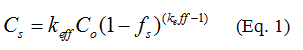
The history of silicon solar cell is more than a half century old. The first Si cell was the end result of producing point-contact rectifiers. Since 1874, sharp metal contact is a suitable candidate to be used with different crystals due to its rectifying properties. Such rectifiers were well known for radio receiver detectors [1]. However, later Si crystal rectifiers were replaced by thermionic tubes. Russel Ohl of Bell Laboratory first prepared polycrystalline Si ingots with junctions from high purity commercial silicon [2]. Figure 1 shows the evolution in terms of efficiency of Si cells starting from 1940. Later in 1941, photovoltaic device physics were well described based on this junction mechanism. Such cells showed almost no photo conversion efficiency. Uncontrollable junction formation found to be main reason for such result. In 1952, Kingsbury and Ohl reported well controlled junction formation [3]. The photo conversion efficiency was around 1%. These early stage findings initiated the full phase deployment of silicon technology also at Bell Laboratories. The first modern Si cell showed a photo conversion efficiency of 4.5% in 1954 developed by Pearson, Fuller and Chapin of Bell Laboratories [4,5]. Subsequently, Fuller succeeded to fabricate a junction made of phosphorus –therefore negatively- doped silicon (n-type c-Si) and boron –therefore positively- doped emitter (p-type c-Si) with 6% efficiency [4,5]. The cell efficiency jumped then to 10% within 18 months [6]. Further enhancement of the efficiency of solar cells with n-type silicon as an absorber was achieved and reached 14% in 1960 [7]. In these 60s years, the main applications of PV cells was the power generation in satellites. It was found indeed that the p-type silicon is less sensitive to the space radiations, such as the Gamma and electrons wind [8]. This discovery triggered the switch to p-type silicon based solar cells.
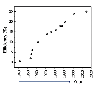
Figure 1. Evolution of the PV efficiency (%) of Si solar cells. Data collected and adapted from Ref. [18].
Since then, boron doped silicon became the material of choice to design the absorbing layer of solar cells. However, by the end of the 90s years, it was established that the presence of Fe-B pairs reduces drastically the photocarrier lifetime, and consequently the efficiency of PV devices. In fact, n-type materials have higher minority-carrier lifetimes because of the absence of oxygen-boron defects [9], and lower capture cross sections of most interstitial 3d transition metals [10], and therefore higher tolerance to common impurities like Fe or O [11]. The return of interest in n-type silicon is due to its potential for the fabrication of high efficiency solar cells [12,13]. Enhancing the performance of the cells is one of the most impactful way to reduce the cost of the energy produced by PV technology. During the last few years, n-type solar cell concepts [9] for industrial use have been successfully reported, yet they are still concentrated on mono-crystalline Si material.
In spite of this fact, almost 85% of the silicon solar cells produced by the industry is still based on p-type substrates, which seems to be dictated by the current cost of the n-type based technology. This high cost is due to several factors, the main one being the absence of large-scale fabrication tools due to the insufficient development and industry implementation of the n-type cell processes, which is in turn for a large part due to a poor development of an industrial low cost technique for passivation of p+ emitters. However, according to a recent report in 2014, a clear shift to n-type substrates is expected [14]. Two solar cell manufacturers, namely SunPower [15] and Sanyo (now Panasonic) [16] have already initiated to manufacture high efficiency commercialized solar cell using n-type crystalline silicon substrates. Panasonic holds the impressive efficiency record of 25.6% at the lab scale [16]. The market share of n-type silicon modules is still small (< 8% in 2014). However, the shift of the photovoltaic industry to the n-type silicon is clear as an increasing number of manufacturers are offering n-type based solar panels. The ITRPPV roadmap projects that the n-type silicon technology will reach a market share higher than 30% by 2021 [17].
From scientific and technological point of view, the design of solar cells using n-type silicon of high performance requires to address some important issues and face many challenges ranging from the successful growth of high quality silicon crystals (to reduce the carrier recombination and enhance the carrier lifetime) to the fabrication of devices with the minimum tolerable electric losses at various contacts and interfaces.
The number of publications on n-type silicon material for PV has increased markedly in recent years. Figure 2 shows how the number of refereed articles on n-type Si for PV has steadily increased since 1999, based on data collected from Scopus web-based information service. Among all the published review articles on the matter, only 11 review works have been conducted, and to the best of our knowledge, only one article review has been published on 2015. In sum, along with the increase of the number of publications in this area comes the need for a comprehensive review article. The objective of this article is to address this need as well.
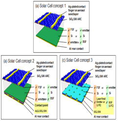
Figure 2. (a) Recent refereed publications related to n-type Si for PV applications, together with (b) their corresponding distribution of subject area and (c) documents types. All published languages were included. All document types, including journal and conference articles, report review, conference proceeding were recorded. Statistics are available from 1999 to March 2015, inclusively. Data were collected from Scopus of peer-reviewed literature web based information service
In this paper, we review some of the main issues related to the n-type silicon based solar cells and the progress made in addressing them. In the first section we compare the effect of impurities on the carrier lifetime in n-type and p-type silicon wafers, the dopant segregation in n-type silicon ingots and some of the solutions proposed to reduce the resistance heterogeneities.
The second part of the paper is dedicated to the description of various cell configurations using n-type silicon as an absorbing layer and the techniques used to optimize their performance.
N-type silicon growth and wafer properties
Impurities and structural defects including dislocations and grain boundaries play a key role in the recombination process of photocarriers which in turn leads to a reduction of cell performance. Defects in boron-doped (p-type) silicon, the dominant crystalline silicon solar cell doping technology, have been widely studied. It is well established that p-type silicon suffers from boron-oxygen defects which cause degradation of most of the solar cell parameters upon illumination [18-24]. The boron-oxygen defect, which can have an energy level near mid-gap [24], is widely believed to be a grown-in point defect which forms a complex of substitutional boron and interstitial oxygen dimer, i.e. BSOi2 complex [22,25]. In oxygen-rich silicon such as Czochralski silicon (CZ-Si), light induced degradation (LID) can be responsible for up to 10% relative efficiency loss [23].
Although n-type silicon does not contain boron-related defects, as opposed to p-type silicon, similar minority-carrier lifetime-limiting grown-in point defects have been recently reported. Rougieux et al., [26,27] and Zheng et al., [28] have observed a de-activation of the defect in high lifetime (millisecond-range) CZ-Si when samples are annealed between 150 and 360 °C. By annealing the as-grown samples at 450°C, an increase in the effective lifetime from ~1.6 to to4.7 ms for 4.1 Ωcm samples, [27] and from 2to 3.4 ms for 0.7 Ω cm samples [28] was achieved at an injection level of Dp=1.0 x 1015 cm-3. This shows that the defects which are suspected to be oxygen and phosphorus vacancy related complexes are highly detrimental to the minority-carrier lifetime in as-grown samples. The defects may have little or even no impact for conventional (or standard, see Section 3) solar cell architectures as they are already annealed-out thanks to the emitter diffusion and contact firing high temperature steps, which is not the case for the low-temperature solar cell fabrication processes.
In addition to the absence of the boron-oxygen defects in phosphorus-doped, n-type c-Si shows better tolerance to lifetime limiting metallic impurities. The capture cross-section (one of the most important parameters of recombination) of interstitial metallic contaminants namely Fe, Ti, Mn, V and Mo, (Table 1 and Figure. 3), is much higher for electrons than for holes. Interstitial iron (Fei) for example, the main lifetime limiting metal impurity in silicon solar cells, has an electron-capture cross-section (σn) which is nearly three orders of magnitude higher than the hole-capture cross-section (σp). At low injection level, the collected photocurrent is controlled by the diffusion/ recombination process of minority carriers. The defect-limited minority carrier diffusion length and therefore Shockley-Read-Hall (SRH) recombination lifetime is thus expected to be higher for n-type than for p-type silicon. This has been verified experimentally in both monocrystalline silicon [29] and in multicrystalline silicon [30-31]. Indeed, very high lifetimes, in the millisecond range required for high efficiency cells have been achieved in n-type silicon, including in multicrystalline silicon [32], mono-like silicon [33] and non-contact crucible silicon [34]. A comparison of lifetimes measured in n-and p-type silicon for various studies is given in Table 2 and summarized in Figure. 3.
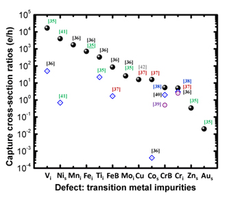
Figure 3. Ratio ofcapture cross-section of electrons to that of holes for most common transition metal impurities in solar cell silicon with respect to the corresponding references.
Table 1. Capture cross-section of electrons and holes for most common transition metal impurities in solar cell silicon. Blanc case means that the defect energy level was not provided.
|
Defect
|
Energy (eV)
|
σn (cm2)
|
σp (cm2)
|
σn/σp
|
Reference
|
|
Fei
|
Ev+0.38
|
5.0 x 10⁻¹⁴
|
7.0 x 10⁻¹⁷
|
714.3
|
[35-36]
|
|
FeB
|
Ec-0.26
|
6.0 x 10⁻¹⁵
5.0 x 10⁻¹⁵
|
7.0 x 10⁻¹⁷
3.0 x 10⁻¹⁵
|
85.7
1.7
|
[36]
[37]
|
|
Cri
|
Ec-0.24
Ec-0.24
|
2.4 x 10⁻¹⁴
2.0 x 10⁻¹³
2.0 x 10⁻¹⁴
|
8.0 x 10⁻¹⁵
8.0 x 10⁻¹⁴
4.0 x 10⁻¹⁵
|
3.0
2.5
5.0
|
[38]
[36]
[37]
|
|
CrB
|
Ev + 0.27
Ev + 0.28
Ev + 0.27
|
3.8 x 10⁻¹⁴
0.5 x 10⁻¹⁴
2.0 x 10⁻¹⁴
|
7.0 x 10⁻¹⁵
1.0 x 10⁻¹⁴
1.0 x 10⁻¹⁴
|
5.4
0.5
2.0
|
[38]
[39]
[40]
|
|
Vi
|
Ev +0.36
|
1.0 x 10⁻¹⁶
5.0 x 10⁻¹⁴
|
2.0 x 10⁻¹⁸
3.0 x 10⁻¹⁸
|
50.0
16666.7
|
[36]
[35]
|
|
Tii
|
Ec-0.27
|
1.0 x 10⁻¹⁴
3.1 x 10⁻¹⁴
|
3.0 x 10⁻¹⁷
1.4 x 10⁻¹⁵
|
333.3
22.0
|
[36]
[35]
|
|
Moi
|
Ev +0.28
|
1.6 x 10⁻¹⁴
|
6.0 x 10⁻¹⁶
|
26.0
|
[35-36]
|
|
Mni
|
|
3.5 x 10⁻¹⁵
|
2.0 x 10⁻¹⁸
|
1750.0
|
[36]
|
|
Nis
|
Ec-0.40
Ev+0.19
|
5.6 x 10⁻¹⁷
4.0 x 10⁻¹²
|
8.0 x 10⁻¹⁷
1.0 x 10⁻¹⁵
|
0.7
4000.0
|
[41]
[41]
|
|
Cu
|
Ec-0.50
|
1.6 x 10⁻¹⁸
|
1.0 x 10⁻¹⁹
|
16.0
|
[37,42]
|
|
Aus
|
Ec-0.55
|
1.4 x 10⁻¹⁶
|
7.6 x 10⁻¹⁵
|
0.02
|
[35]
|
|
Cos
|
Ev+0.41
|
2.0 x 10⁻¹⁵
1.6 x 10⁻¹⁴
|
5.0 x 10⁻¹⁸
1.0 x 10⁻¹⁵
|
0.0004
16.0
|
[36]
[37]
|
|
Zns
|
Ev+0.33
|
1.5 x 10⁻¹⁵
|
4.4 x 10⁻¹⁵
|
0.34
|
[35]
|
Table 2. Comparison of minority carrier lifetimes estimated at typical excess carrier concentration D= 1.0 x 1015 cm-3 in p-type ( ) and n-type ( ) silicon in similar materials and processing (in the respective study)
|
tp(μs)
|
tn(μs)
|
tn/tp %
|
Notes
|
Ref.
|
|
|
|
|
|
|
|
17.6
|
3.2
|
18.2
|
tCr: (Associated)
|
[38]
|
|
17.6
|
8.2
|
46.6
|
tCri: (100% dissociated)
|
[38]
|
|
300.0
|
40.0
|
13.3
|
tFei
|
[35]
|
|
9000.0
|
2000.0
|
22.2
|
FZ-Si
|
[43]
|
|
190.0
|
50.0
|
26.3
|
MC-Si
|
[44]
|
|
1300.0
|
400.0
|
30.8
|
Compensated Si with
defects annihilated
|
[45]
|
|
200.0
|
20.0
|
10.0
|
Compensated Si with
defects generated
|
[45]
|
|
50.0
|
4.0
|
8.0
|
tFei: As-grown
|
[46]
|
|
160.0
|
110.0
|
68.7
|
tFei: Gettered and passivated
|
[46]
|
|
554.5
|
100.0
|
22.0
|
FZ-Si, SRH and Emitter recombination (Simulated)
|
[47]
|
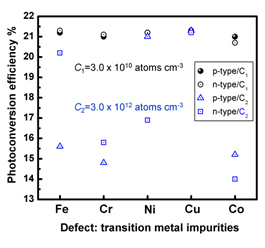
Figure 4. Photoconversion efficiency comparison in metal contaminated n- and p-type solar cells estimated from Ref. [48] at defect concentration C1= 3.0 x 10¹⁰ atoms/cm3 and C2= 3.0 x 10¹² atoms/cm3.
However, many questions still remain, regarding the effect on recombination of metallic impurities in n-type silicon. Recent numerical modelling using 2-D SENTAURUS on high efficiency passivated emitter rear cell and structure (PERC –different cell structures will be detailed insection 3 below), and more recent values for recombination parameters show that the interstitial species Fei and slightly Cri are indeed more detrimental to conversion efficiency in p-type silicon while the substitutional species Cu, Ni and Co are more detrimental in n-type silicon, [48]. Figure 5 shows the impact of metal contamination on n- and p-type solar cells estimated from the study at defect concentration 3.0 x 10¹⁰ atoms/cm3 and 3.0 x 10¹² atoms/cm3 (Industrial multicrystalline silicon contains much higher concentration of these impurities [49].
At low concentration, the overall impact of the metal species on photoconversion efficiency and the variation on how a given specie affects the n- or p-type material is small. At high concentration, in this case, two orders of magnitude higher, the impact on efficiency is high and the variation in how each metallic-specie affects the n- or p-type silicon is apparent. It should be noted that the effect of structural defects (discussed below) was not taken into account and the metal species were assumed to be dissociated. Recently, Sun et al., [50] have investigated a particular case of Cr, comparing its effect on SRH recombination lifetime in p- and n-type silicon with similar doping and concentration of Cr. N-type silicon was found to have higher lifetimes in all cases, i.e. when Cr was 100% dissociated, partly or fully associated. The CrB defect was found to be more recombination active than Cri as shown in Figure 3.
In low-cost multicrystalline silicon, the most detrimental impact on minority-career lifetime is rooted on the presence of extended structural defects, i.e. dislocations and grain boundaries. It has been reported that clustered extended defects can be responsible for the loss of conversion efficiency of up to 4% absolute [51]. Extended defects are prominent in crucible-grown directionally solidified silicon, which is the main low-cost path for growing solar cell silicon, including mono-like silicon, conventional and high performance multicrystalline silicon (mc-Si). The majority of the defects are grown-in defects. Post-growth processing schemes such as junction formation, contact firing at high temperature or by laser-scribing and/or firing can induce additional defects, including surface damage, stacking faults and dislocations. Extended defect areas are energetically favourable sites for impurity precipitate nucleation and growth. Consequently, dislocation clusters and grain boundaries play an important role in the precipitation of metallic impurities during crystal growth and cooling. While precipitation at defect sites is partly advantageous due to internal gettering, creation of metal impurity reservoirs is undesirable. Furthermore, the defects may undermine external gettering, which is more important, as well as aid in homogeneity in the distribution of dopants. Several studies have compared the impact of structural defects on n- and p-type silicon. Cotter et al., [52] have studied the effect of processing-related defects such as boron diffusion-induced misfit dislocations, laser scribe-induced dislocations and laser scribe-induced surface damage, and observed that n-type silicon was much more tolerant to introducing the defects as well as to the presence of the induced defects, giving much higher lifetime than p-type silicon.
One of the drawbacks of n-type silicon is the distribution of the dopants during crystal growth. Disregarding solid state diffusion, the distribution of a given impurity specie in directionally solidified silicon depends on its effective segregation coefficient, ( ), given by the Scheil equation:
Where is the volume fraction solidified, Cs the concentration of the impurity specie in the solid and is the initial concentration in the melt. The effective segregation coefficients forboron and phosphorus in silicon are 0.8 and 0.35, respectively [53]. Consequently, n-type ingots suffer from undesirable variation in resistivity along the ingot height, unlike p-type silicon whose distribution is rather homogeneous.
In homogeneity in resistivity due to segregation of dopants to structural defects has also been a concern for n-type silicon. Mandurah et al.,[54] and Carabelas et al. [55], studied various dopants, like phosphorus (P), arsenic (As) and boron (B), implanted in polycrystalline silicon films, by annealing the samples in the temperature range 700 -1000 . The measurements of the active dopants as a function of the temperature in the bulk and in grain boundaries have revealed grain boundary segregation for phosphorus and arsenic, but not for boron. Such a segregation can result in variation in the bulk resistivity caused by the reduction in the concentration of dopants, as was indeed observed the mentioned studies as well as that achieved by Wong, et al.,[56], in the case of arsenic. Segregation to the defects can also cause change in defect states and defect structure which may modify recombination behaviour of the structural defects, precipitated metallic impurities and point defects. The segregation of phosphorus to grain boundaries and dislocation clusters and the impact on electrical propertiesis yet to be investigated thoroughly in solar cell silicon.
Gettering and passivation are important processes for improvement of the electrical properties of crystalline semiconductors.
- Gettering is a high temperature process, which involves dissolution of the precipitates and diffusion of the point defects towards the gettering layer. Phosphorus or boron diffusion steps in standard solar cell process are efficient gettering schemes. However, gettering in areas of high structural defect density is generally ineffective [57], and may lead to contamination and deterioration of the surrounding local regions [58] or even the overall electrical performance of the wafer/cell [59].
- Passivation renders surfaces and to some extent interface and bulk defects electrically inactive, by for example bonding of dangling bonds to hydrogen during SiNx:H antireflection coating deposition.
Several studies have compared the effectiveness of gettering and passivation in n- and p-type multicrystalline silicon. Coletti et al.,[31] studied the effect on silicon intentionally contaminated with iron (by addition of 53 ppm by weight of iron in the feedstock) and found that lifetime improvement with phosphorus gettering and hydrogenation could be up to 50 times in p-type silicon and only up to 5 times for n-type silicon. Deterioration in lifetime in intra-grain areas where the as-grown lifetime was high was also observed. Geerligs et al.,[59] studied the effect of the same on industrial-representative wafers. The study found that grain boundaries and dislocation clusters become more recombination active after gettering in both n- and p-type wafers. However, while a net reduction in the electrical activity of the crystal defects was achieved for p-type silicon after hydrogen passivation of the gettered wafers, the combined gettering and passivation scheme was not beneficial for the n-type silicon, such that processed lifetimes was similar to as-grown lifetimes. In general, it is now well established that the recombination activity of Ni, Co and Cu increases on formation of precipitates or upon decoration of structural defects, as extensively reviewed by Istratov et al., [60]. It appears therefore that metallic impurity precipitation at crystal defects during growth or high temperature processing is equally or even more detrimental to the performance of solar cells made of n-type silicon. These results indicate that the reduction of extended defects is critical for the design of solar cells of high efficiency using n-type silicon. The growth of mono like silicon ingots is a promising cost effective and potentially R&D path to avoid the presence of grain boundaries. However, the reduction of the dislocations density to values below 104 cm2/sis required to obtain silicon wafers of ms lifetime. This requires a careful control of the temperature gradient in the furnace during growth as it generates thermal stresses and plastic deformation of silicon [61-62].
The shift to n-type silicon for the design of solar cells of high efficiency does not only require the optimization of the electrical properties of the wafer but also the design of a device that minimizes the current losses. We describe in the following section the different cell designs and the issues raised by the use of n-type silicon as an absorbing layer.
For n-type solar cells to compete with the current p-type ones, the ultimate figure of merit would be the cost per unit of energy produced. At the cell level, this means that devices have to be fabricated with higher efficiency and lower (or comparable) costs. Generally, two approaches could be considered to design a fabrication process that is suitable for n-type based cells. Some authors suggest adjusting the p-type cell processing to the n-type material. Others suggest introducing new processes and cell architectures taking into account the n-type material specific properties.
In the following section, we describe the main solar cell fabrication processes that use n-type crystalline silicon as a base (absorber) material. First, we discuss the processing of n-type material using similar process steps used in the fabrication of the conventional screen-printed aluminum back surface field (Al-BSF).Next, various passivated emitter and rear cell architectures are reviewed. The pros and cons of the various cells architectures yielded by each cell processing technology will be presented. Then, we discuss the potential of silicon heterojunction (SHJ) and interdigitated back contact cells (IBC) as promising devices based on n-type silicon.
This technology path takes advantage of using the same process as the main product on the crystalline silicon PV market: the so-called “Al BSF” solar cell. The latter is based on p-type wafers for which the emitter is diffused with phosphorous at the front, and the back is screen-printed with Al that serves both as a back contact, and for making a back surface field. In the case of an n-type wafer, the same phosphorous diffusion is now creating a Front Surface Field (FSF), whereas the screen-printed aluminum that made the back surface field creates now an emitter, the resulting structure is shown for both cases on Figure 5 (a). Given that in this concept the junction is at the rear for the n-type wafer, the separation of the generated carriers in the bulk has to happen toward the backside of the cell, whereas most of the carriers are photogenerated towards the front, so the diffusion length of the minority carriers needs to be sufficient to reach the back, and the quality of the wafer plays a crucial role. Fraunhofer ISE reached about 19.3% efficiency [63] using n-type float-zone wafers; similar efficiencies were reached also by the PANDA solar cells of Yingli solar [64].Amongst the best efficiencies reached on small area according to S. Glunz [65] was 19.8% [66] with a Voc of 640 mV. This process is not expected to bring record efficiencies, because of the absence of passivation of the contacts that are an important cause of carrier recombination, It is however the closest to be adopted for mass production.
The direct contact of metals with silicon is usually an important source of trap-assisted recombination through Shockley-Read-Hall (SRH) process. Therefore concepts involving passivation of the rear contacts as well as of the front emitter arose. Improving the emitter passivation was achieved through adding a thin thermal oxide layer between the silicon nitride antireflection coating and the emitter layer, which is currently achieved as well in standard commercial Al-BSF crystalline silicon solar cells [67] (Figure 5 a). Passivating the back contact involves adding an intermediate dielectric layer between the silicon and the back metallic surface, with the good side effect of enhancing thereby the reflection on the back side. It however involves making holes in this dielectric layer in order to ensure the physical and then electrical contact between the metal and the base silicon. This gave birth to the PERC concept (Passivated Emitter and Rear Cell) (Figure 5 b). However, the cell concept that held the record efficiency in silicon solar cells has long been the PERL one (Passivated Emitter and Rear Locally Diffused Concept of the Australian National University, with 25% efficiency [67], where, added to the back side passivation and the restriction of the metal-silicon contact to a collection of single points, these remaining contact areas were passivated by the local diffusion of a doping creating a supplementary surface field (Figure 5 c).
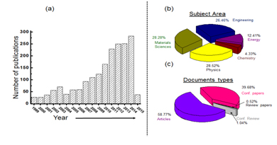
Figure 5. Schematic showing various cell concepts in two declinations: n or p type base,(a) full Al back, (b) passivated emitter and rear, (c) passivated emitter and locally diffused rear. Adapted from Ref. [68].
The exact transfer of this successful concept from p- to n-type is not as straight-forward than in the case of the Al-BSF concept. Various modifications were needed to be made. Figure 6 shows the transfer of the PERL fabrication process flow from p to n-type by IMEC (Leuven, Belgium) [68] while keeping as much as possible common process steps, in order to minimize the added costs, giving birth to the n-PERT (Passivated Emitter and Rear Totally diffused concept), where the junction passes from front to back (as for the Al BSF concept transfer from p to n described above). One can notice that a slight increase in the number of process steps is necessary, balanced by an efficiency improvement. However, a detailed cost analysis has to be made in order to evaluate precisely the economic advantage of such process. Figure 7 shows a schematic of the two cell architectures, namely the p-type passivated emitter and rear locally diffused (p-PERL) cell with aluminum-alloyed localized p+ back-surface (BSF) and homogenous 120 Ω/sq n+ front emitter (Figure. 7a), and the n-type passivated emitter and rear totally diffused (n-PERT) cell with blanket p+ rear emitter and homogenous 120 Ω/sq n+ front surface field (Figure 7b). Both cells make use of self-aligned Ni/Cu/Ag front side plated contacts.
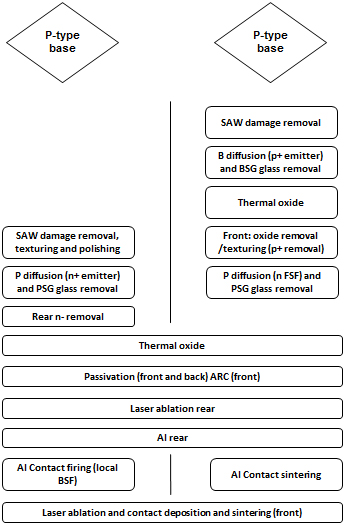
Figure 6. Similarities and differences for the passivated emitter and rear concepts when switching from p to n-type c-Si base. Adapted from Ref. [68].
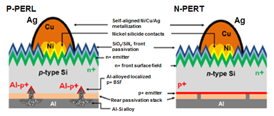
Figure 7. Schematic of (a) p-type passivated emitter and rear locally diffused (p-PERL), and (b) n-type passivated emitter and rear totally diffused (n-PERT) cell. Both cells make use of self-aligned Ni/Cu/Ag front side plated contacts.
In the same work by IMEC, an interesting power loss analysis comparison was performed on the (p-) PERL and n-PERT concepts; the main result of the analysis is reproduced here on Figure 8. One can clearly see the effect of the higher tolerance to defects of an n-doped base material: whereas doping is similar, the recombination losses are smaller.
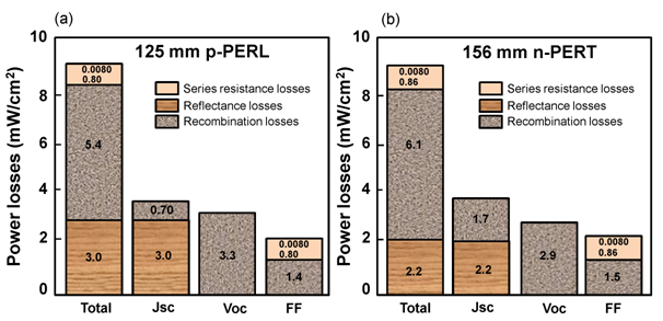
Figure 8. Power loss analysis of (a) the best 125 mm p-type passivated emitter and rear locally diffused (p-PERL) and (b) the best 156 mm n-type passivated emitter and rear totally diffused (n-PERT) cells.
SHJ cells are based on a bulk crystalline silicon base absorber on which thin layers of amorphous silicon are deposited: doped layers serving as an emitter or a surface field, and intrinsic layers serving as surface and contact passivating layers. The most famous concept of SHJ is the heterojunction with intrinsic thin layer (HIT) solar cell configuration was developed by Sanyo (presently Panasonic) 30 years ago [69]. This design allows high conversion efficiencies at the industrial level. The high conversion is mostly allowed by the passivation of the contacts offered by the intrinsic layer of hydrogenated amorphous silicon,. As De Wolf et al. mentionedin their review [70]: [The key feature of this technology is that the metal contacts, which are highly recombination active in traditional, diffused-junction cells, are electronically separated from the absorber by insertion of a wider bandgap layer. This enables the record open-circuit voltages typically associated with heterojunction devices without the need for expensive patterning techniques].
Note that given the fact the SHJ cells find their first justification in the quest for high efficiency silicon solar cells, in particular through a high open circuit voltage (Voc), the cost aspect has never been a crucial aspect. Manufacturers (Only Sanyo-Panasonic at a commercial level for the moment) have therefore immediately started using n-type wafers despite their higher cost, in order to ensure the best material possible and the highest robustness to defects.
Descoeudres et al. have performed a unique study using the same fabrication processes [71]. They fabricated and compared SHJ cells based on n- and p-type crystalline silicon, using both Czochralski (Cz, used in industry) and Float zone (FZ, high-quality) silicon wafers, in two different configurations where the junction is at the front or at the back. The structure obtained is shown in Figure 9.
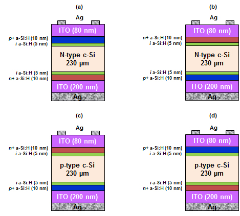
Figure 9. The schematic is showing different heterojunction solar cell structures tested (not to scale). (a) n-type wafer with front emitter. (b) n-type wafer with rear emitter. (c) p-type wafer with front emitter, and (d) p-type wafer with rear emitter.
It is then found that the same tendency of the superiority of the n-type cells comparatively to the p-type ones is also maintained in the case of SHJ. This is mainly due to the fact that n-type c-Si is more tolerant to defects, as earlier discussed in this paper, and, on the other hand to the “band structure seen by minority carriers” [71] that yields a very different behavior at low injection levels. This means that the lifetime of minority carriers in p-type CZ-Si is much lower than that in the n-type below a minority carrier density of 1016/cm3. However, on high-quality FZ wafers with a very low defect density, this difference between n and p type disappears, showing that the SHJ concept is able to provide the sufficient surface passivation, if the bulk quality is high enough. Indeed, in diffused emitter cells, the highest recombining zone is the highly doped emitter; SHJ cells overcome this limitation by improved surface and interface passivation, while bulk lifetime becomes more important. Some recent developments have proposed to combine both worlds, i.e., the diffused emitter (with less absorption losses) and the passivated contact (avoiding surface recombination) [72].
Another promising technique to enhance the cell efficiency is by avoiding the shading due to the front contacts. All the contacts are then on the rear side. Hence light absorption is enhanced by reducing the shading effect [73]. However, carrier diffusion length needs to be very high for this structure, as all photo-generated carriers need to be collected from the rear side. This structure features two critical advantages, first, it decreases the recombination rate near the contact –thanks to a smaller silicon-metal contact area-, and second, it improves the light trapping. The best cell efficiency reached with such a structure is the record 25% of Sunpower on n-type c-Si [74]. Given the importance of the diffusion length of minority carriers, with such a contacting scheme, the use of n-type c-Si is here crucial. Several industrial and academic laboratories are currently working on this concept.
In this section, the role of defects and impurities during solar cell fabrication will be discussed, with a focus on the two most sensitive steps: junction formation and passivation. The fundamental impact of defects and impurities of different n-type solar cell architecture will be highlighted. Besides carrier recombination linked to the bulk material quality that were discussed above, the two main factors of losses that need to be tackled when designing a crystalline silicon solar cell are surface recombination and incomplete light absorption. Bulk recombination is due to the bulk defects. As for light absorption: crystalline silicon has - regardless of its doping- a low absorption coefficient on a relatively broad spectrum. Light trapping will not be discuses in details here. The focus is on emitter passivation. Surface recombination contributes significantly to the current loss because of the long carrier lifetimes and therefore long diffusion lengths. Carriers can reach easily the surface and recombine before being collected, thus the need for surface passivation. Other factors such as resistive losses are also present. The most successful designs reaching record efficiencies are designs where passivation and light trapping are combined, with some variations in the junction and surface field formation processes.
N-type material requires boron doping using either boron tribromide (BBr3) diffusion process or a liquid boron source. Depending on the cell processing, this can be done using different doping techniques ranging from standard BBr3 diffusion process at relatively high temperature [75-76] to the deposition of boron silicate glass (BSG) layer by atmospheric pressure chemical vapor deposition (APCVD) [77]. However, it is worth noting here that boron diffusion requires higher temperature and longer diffusion time as compared with phosphorus diffusion, due to its lower diffusivity in silicon. During the diffusion process, formation of boron rich layer (BRL) occurs, which acts as a dead layer, similar to the phosphor silicate glass (PSG) in p-type cells, and needs to be removed completely since SRH recombination is generally correlated with the presence of this inactive layer [78-79].
Ion implantation is mainly used in the microelectronics industry and well-established technique to fabricate complementary metal oxide semiconductor (CMOS) devices. It is thought to be another promising fabrication technique to fabricate n-type based solar cells. Such technique gives the control over single side growth mechanism. Interdigitated back contact (IBC) and selective emitter could be the best choice to be done using this technique. Ion implantation can help to form n+ or p+ doped emitters. Less doping ions are needed for such technology. A large area manufacturing is possible using ion implantation technique [80]. The correct doping profile as well as uniformity of emitters needs to be controlled. High bombardment rate due to ion implantation could etch the surface passivation layer, which later on can be reproduced by annealing. However, annealing could increase the diode saturation current. A research work in Fraunhofer ISE showed very low dark saturation current for boron-doped emitters [81,82]. Such technique also enables in-situ masking of implantation. The advanced cell processing technique can be more simplified by ion implantation method as a state of the art technology. It reduces processing steps, improvement of cell absorption to longer wavelength, edge isolation elimination. The collaborative work of Sunvia Inc., Varian Semiconductor Equipment Associates (VSEA) and the Georgia Institute of Technology successfully fabricated such cells with 19.1% efficiency [83].
A good surface passivation of n-type material with a front boron emitter is required for high efficiency cells. Different passivation techniques are used to passivate the front and rear surfaces of n-type solar cell materials by reducing defect densities. However, the aim here is to achieve a combination of an excellent passivation properties and a low fabrication process cost.
Amorphous hydrogenated Silicon nitrides a-SiNx:H is known to passivate bulk defects in p-type Aluminum Back Surface Field (Al-BSF) solar cells by passivating the silicon dangling bonds. Plasma Enhanced Chemical Vapor Deposition (PECVD) process at temperature around 350 °C is used to deposit this layer. However, SiN:H does not work properly to passivate the front boron emitter in n-type solar cells [84].
In PERC type solar cells made of moonlike silicon material, thermal oxidation showed improved passivation properties that reduce the dislocation density without negative impact on bulk lifetime [85]. A stack of silicon dioxide (SiO2) and hydrogenated silicon nitride (SiNx:H) was used for surface passivation for both n-type (as opposed to silicon nitride alone) and p-type material [86-89]. PECVD is used to deposit the SiNx:H, while SiO2 is deposited thermally. A high temperature (above 1000 °C) is required for oxide thermal passivation of SiO2, which is responsible for reducing defects at the silicon interface.
Intrinsic hydrogenated amorphous silicon (i) a-Si:H from the other hand showed excellent passivation properties for SHJ solar cells [90-91]. The film is deposited generally using PECVD at relatively low temperature process around 200 °C and resulted hydrogenation of silicon dangling bonds resulting in reduction of interface defect density [92].
Finally, aluminum oxide Al2O3 is being considered as a good passivating layer thanks to the high fixed negative charge density at the silicon and Al2O3 interface that ensures effective field-effect passivation [93-94]. Al2O3 layer passivation is suitable for both back-side of p-type solar cells and boron emitter of n-type solar cells. Lee et al. [95] reported on a low emitter saturation current of 38 fA/cm2 due to a stack of Al2O3/TiO2 used as a front passivating and antireflective layers in an n-type cell configuration. Various techniques were used to deposit Al2O3 film with similar passivation properties, e.g., atomic layer deposition (ALD), PECVD and APCVD. The tradeoff in process selection in industry is the deposition rate and the need for vacuum.[Tables 3 and 4]
Table 3. Best efficiencies reported for the different types of solar cell [18]
|
Cell type
|
Highest reported efficiency for small area cells produced in the laboratory
|
Highest reported module
efficiency
|
|
c-Si (monocrystalline Si)
|
25.6% (University New South Wales, passivated emitter with rear locally diffused Panasonic, IBC-SHJ)
|
22.7% (University New South Wales /Gochermann)
|
|
Multi-c-Si
|
20.3% (Fraunhofer Institute for Solar Energy Systems ISE)
|
15.3% (Sandia/heat exchanger method)
|
|
aSi:H, amorphous Si
|
10.2% (Fraunhofer Institute for Solar Energy Systems ISE), 15.3% (Sandia/heat exchanger method)10.1% (Kaneka),
N.B. single junction
|
Triple junction. Stabilized
efficiency: 10.4%
|
Table 4. Best results for various n-type high efficiencies cell structures
|
Type
|
Structure
|
Metallization
|
Voc (mV)
|
ƞ (%)
|
Ref.
|
|
Front surface field (FSF) rear emitter cells
|
n+np+PERT (rear emitter cell)
|
Plated Ag
|
702
|
22.7
|
[96]
|
|
n+np+ (Al rear emitter)
|
Front evaporated Ti/Pd/Ag. Rear full area evaporated
|
649
|
20.1
|
[97]
|
|
n+np+ (back contacts)
|
Screen printed
|
647
|
20
|
[98]
|
|
Back surface field (BSF) front emitter cells
|
IBC
|
|
721
|
24.2
|
[99]
|
|
PERL (p+nn+)
|
Evaporated front grid, Rear full area evaporated
|
705
|
23.9
|
[100]
|
|
PERL (p+nn+)
|
Evaporated front grid + Plating, rear full area evaporated
|
695
|
21.9
|
[101]
|
|
(p+nn+) PANDA CEll
|
Stencil printed
|
649
|
20
|
[102]
|
|
MWT (p+nn+) back contacts
|
Stencil printed
|
644
|
19.7
|
[103]
|
|
Heterojunction with intrinsic thin layer (HIT) solar cell
|
HIT Cell
|
Screen printed
|
745
|
23.7
|
[104]
| 2021 Copyright OAT. All rights reserv
|
Ion implanted emitter cells
|
IBC
|
Evaporated Al/Ti/Pd/Ag
|
650.1
|
20
|
[105]
|
Conclusions
The growing interest for n-type silicon as an absorbing layer in solar cells is mainly motivated by the need for devices of higher efficiency as an effective way to reduce the cost of the energy produced by PV technology. However, the shift from p-type silicon based to n-type based solar cells requires to address different issues related to the growth of the material as well as the adaptation of the fabrication process of the solar cells.
In order to fully take advantage of the better tolerance of the n-type c-Si material, the growth of the material has to be taken carefully.
Indeed, we have seen how impurities and structural defects including dislocations and grain boundaries played a key role in the recombination process of photocarriers which in turn leads to a reduction of cell performance. While the p-type silicon suffers from boron-oxygen defects which cause degradation of most of the solar cell parameters upon illumination, the n-type silicon does not contain boron-related defects, as opposed to p-type, in addition it shows better tolerance to lifetime limiting metallic impurities. The shift to n-type silicon for the design of solar cells of high efficiency does not only require the optimization of the electrical properties of the wafer only but also the design of a device that minimizes the current losses.
For the fabrication of n-type c-Si based cells with a diffused emitter (Full Al or passivated back surface) that are presently dominating the market, the fabrication of solar cells is mostly being done by mimicking as much as possible of the p-type, allowing to expect no increase of the fabrication costs when going to industry. Some steps required some modifications (such as the transition from PERL to PERT, with a back surface totally diffused in order to ensure a full area junction, instead of the local diffusion of the surface field) and their development therefore needs some time. Once the adaptation is fully controlled, given that no disruptive or qualitative change was needed, one can expect to reach better efficiencies with an n-type wafer as a base material than with p-type.
On the other hand, SHJ solar cells are already fabricated on n-type silicon solar cells and have recently reached record efficiencies when combined with the IBC concept. However, as we have seen, in order for the n-type silicon to give its full potential with SHJ, a good quality material is needed.
For all the types of fabrication paths mentioned here, no drastic cost increase in the cell processing is expected by the use of n-type c-Si. The most important increase in the fabrication cost is actually due to the n-type c-Si wafer itself: due to the small amount of such wafers presently fabricated, the economy of scale is much smaller than for p-type, an issue that should be resolved soon, given the industry’s present trend.
References
- Braun (1874) On conductance in metal sulphides. Ann Phys Lpz 153, 556.
- Ohl RS (1941) Light-sensitive electric device US Patent 2402622, filed 27 March 1941; 1941 Light-sensitive device including silicon US Patent 2443542, 27, May.
- Kingsbury EF, Ohl RS (1952) Photoelectric properties of ionically bombarded silicon. Bell Syst Tech J 31: 802.
- Chapin DM, Fuller CS, Pearson GL (1954)A new silicon p-n junction photocell for converting solar radiation into electrical power. J Appl Phys 25: 676
- Pearson GL (1985) PV founders award luncheon Conf. Record 18th. IEEE Photovoltaic Specialists Conference, Las Vegas.
- Bell Labs (1954) Record November, 436; 1955 Bell Labs. Record May: 166.
- Mandelkom J, McAfee C, Kesperis J, Schwartz L, Pharo W (1962) Fabrication and characteristics of phosphorus-diffused silicon solar cellsJ. Electrochem. Soc109: 313.
- Green MA(1993) Silicon solar cells: evolution, high efficiency design and efficiency enhancements. Semicond Sci Techno1 8: 1.
- Bothe K, Schmidt J (2006) Electronically activated boron-oxygen-related recombination centers in crystalline silicon. J Appl Phys 99, 013701
- Macdonald D, Geerligs LJ (2004) Recombination activity of interstitial iron and other transition metal point defects inp- andn-type crystalline silicon Appl. Phys.s Lett 85: 4061.
- Hieslmair H, Mandrell L, Latchford I, Chun M, Sullivan J (2012) High Throughput Ion-Implantation for Silicon Solar Cells. Energy Procedia 27: 122.
- Glunz SW, Rein S, Lee JY, Warta W (2001)Minority carrier lifetime degradation in boron-doped Czochralski silicon. J Appl Phys 90: 2397.
- Cotter JE, et al. (2015) 15th Workshop on Crystalline Silicon Solar Cells & Modules: Materials and Processes.
- International Technology Roadmap for Photovoltaic (ITRPV 2013).
- SUNPOWER, http://us.sunpowercorp.com/, 2013.
- Sanyo Solar, http://panasonic.net/energy/solar/, 2013.
- ITRPV Edition 2014. International Technology Roadmap for Photovoltaic (ITRPV.net) Results 2013. http://www.itrpv.net/Reports/Downloads/2014/
- GreenMA, Emery K, Hishikawa Y, Warta W, Dunlop ED (2015) Solar cell efficiency tables (Version 45): Solar cell efficiency tables. Prog Photovolt Res Appl 23, 1: 1–9.
- Verlinden P, Deng W, Zhang X, Yang Y, Xiong Z, et al.(2014) Strategy, development and mass production of high-efficiency crystalline silicon pv modules, Pap. 4sMoO14 6th World Conf. PV Energy Convers. Kyoto.
- ITRPV Edition 2015. International Technology Roadmap for Photovoltaic.
- Sopori S, Basnyat P, Devayajanam S, Shet S, Mehta V, et al. (2012) Understanding light-induced degradation of c-Si solar cells, in the proceedings of 38th Photovoltaic Specialists Conference (PVSC), 001115–001120.
- Bothe K, Sinton R, Schmidt J (2005) Fundamental boron-oxygen-related carrier lifetime limit in mono- and multicrystalline silicon. Prog Photovolt Res Appl 287–296.
- Schmidt J (2004) Light-induced degradation in crystalline silicon solar cells. Solid State Phenom 95, 187–196.
- Schmidt, Cuevas A (1999) Electronic properties of light-induced recombination centers in boron-doped Czochralski silicon. J Appl Phys 86: 3175–3180.
- D. Palmer, K. Bothe, and J. Schmidt, Kinetics of the electronically stimulated formation of a boron-oxygen complex in crystalline silicon. Phys Rev B, 76.
- Rougieux FE, Grant NE, Macdonald D (2013) Thermal deactivation of lifetime-limiting grown-in point defects in n-type Czochralski silicon wafers. Phys Status Solidi RRL-Rapid Res Lett 7: 616–618.
- Rougieux FE, Grant NE, Macdonald D (2014)Impact of Grown-in Point-defects on the Minority Carrier Lifetime in Czochralski-grown Silicon Wafers. Energy Procedia 60: 81–84.
- Zheng P, Rougieux FE, Grant NE, Macdonald D (2015)Evidence for Vacancy-Related Recombination Active Defects in as-Grown N-Type Czochralski Silicon, IEEE. J Photovolt 5: 183–188.
- Macdonald D, Geerligs LJ (2004) Recombination activity of interstitial iron and other transition metal point defects in p- and n-type crystalline silicon. Appl Phys Lett 85: 4061.
- Martinuzzi S, Palais O, Pasquinelli M, Barakel D, Ferrazza F (2005) N-type multicrystalline silicon wafers for solar cells, in Photovoltaic Specialists Conference, Conference Record of the Thirty-first IEEE 919–922.
- Coletti G, Kvande RK, Mihailetchi VD, Geerligs LJ, Arnberg, et al. (2008) Effect of iron in silicon feedstock on p- and n-type multicrystalline silicon solar cells, J Appl Phys 104: 104913.
- Cuevas A, Kerr MJ, Samundsett C, Ferrazza F, Coletti G (2002) Millisecond minority carrier lifetimes in n-type multicrystalline silicon. Appl Phys Lett 81: 4952.
- Jay F, Muñoz D, Desrues T, Pihan E, de Oliveira VA, et al.(2014) Advanced process for n-type mono-like silicon a-Si: H/c-Si heterojunction solar cells with 21.5% efficiency. Sol Energy Mater Sol Cells 130: 690–695.
- Kivambe M, Powell DM, Castellanos S, Ann Jensen M, Morishige AE, et al.(2014) Minority-carrier lifetime and defect content of n-type silicon grown by the noncontact crucible method. J Cryst Growth 407: 31–36.
- Macdonald D, Geerligs LJ (2004)Recombination activity of interstitial iron and other transition metal point defects in p- and n-type crystalline silicon. Appl Phys Lett 85: 4061.
- Martinuzzi S, Palais O, Pasquinelli M, Barakel D, Ferrazza F (2005) N-type multicrystalline silicon wafers for solar cells, in Photovoltaic Specialists Conference, 2005. Conference Record of the Thirty-first IEEE, 919–922.
- Schmidt J, Lim B, Walter D, Bothe K, Gatz S, et al.(2013) Impurity-Related Limitations of Next-Generation Industrial Silicon Solar Cells, IEEE. J Photovolt 3: 114–118.
- Sun C, Rougieux FE, Macdonald D (2014) Reassessment of the recombination parameters of chromium in n- and p-type crystalline silicon and chromium-boron pairs in p-type crystalline silicon. J Appl Phys 115: 214907.
- Schmidt J, Krain R, Bothe K, Pensl G, Beljakowa S (2007) Recombination activity of interstitial chromium and chromium-boron pairs in silicon. J Appl Phys 102: 123701–123701–10.
- Habenicht H, Schubert MC, Warta W (2010) Imaging of chromium point defects in p-type silicon. J Appl Phys 108: 034909
- Rein S(2006) Lifetime spectroscopy: a method of defect characterization in silicon for photovoltaic applications, 85. Springer Science & Business Media.
- Macdonald D, Brendle W, Cuevas A, Istratov AA (2002) Injection-dependent lifetime studies of copper precipitates in silicon, Present. 12th Workshop Cryst Silicon Sol. Cells Mater Process. Breckenridge CO 2002.
- Veith B, Ohrdes T, Werner F, Brendel R, Altermatt PP, et al.(2014) Injection dependence of the effective lifetime of n-type Si passivated by Al 2 O 3: An edge effect? Sol Energy Mater Sol Cells 120: 436–440.
- Schmiga C, Schmidt J, Ghosh M, Metz A, Hezel R (2004) Gettering and passivation of recombination centres in n-type multicrystalline silicon, in the proceedings of 19th European Photovoltaic Solar Energy Conference.
- Lim B, Rougieux F, Macdonald D, Bothe K, Schmidt J (2010)Generation and annihilation of boron–oxygen-related recombination centers in compensated p- and n-type silicon. J Appl Phys 108: 103722.
- Coletti G, Kvande R, Mihailetchi VD, Geerligs LJ, Arnberg L, et al.(2008) Effect of iron in silicon feedstock on p- and n-type multicrystalline silicon solar cells. J Appl Phys 104: 104913.
- Cotter JE, Guo JH, Cousins PJ, Abbott MD, ChenMW, et al. (2006) P-Type Versus n-Type Silicon Wafers: Prospects for High-Efficiency Commercial Silicon Solar Cells. IEEE Trans. Electron Devices 53: 1893–1901.
- Schmidt J, Lim B, Walter D, Bothe K, Gatz S, et al. (2013) Impurity-Related Limitations of Next-Generation Industrial Silicon Solar Cells, IEEE. J Photovolt 3: 114–118.
- Istratov AA, Buonassisi T, McDonald RJ, Smith AR, SchindlerR, et al. (2003) Metal content of multicrystalline silicon for solar cells and its impact on minority carrier diffusion length. J Appl Phys 94: 6552.
- Sun C, Rougieux FE, Macdonald D (2014) Reassessment of the recombination parameters of chromium in n- and p-type crystalline silicon and chromium-boron pairs in p-type crystalline silicon. J Appl Phys 115: 214907.
- Sopori B, Rupnowski P, Mehta V, Budhraja V, Johnston S, et al.(2009) Performance limitations of mc-Si solar cells caused by defect clusters. ECS Trans 18: 1049–1058.
- Cotter JE, Guo JH, Cousins PJ, Abbott MJ, Chen FW, et al. (2006) P-Type Versus n-Type Silicon Wafers: Prospects for High-Efficiency Commercial Silicon Solar Cells IEEE Trans Electron Devices 53: 1893–1901.
- Davis JR, Rohatgi A, Hopkins RH, Blais PD, Rai-Choudhury P, et al.(1980) Impurities in silicon solar cells, IEEE Trans. Electron Devices 27: 677–687.
- Mandurah MM, Saraswat KC, Helms CR, KaminsTI, et al.(1980) Dopant segregation in polycrystalline silicon. J Appl Phys 51: 5755–5763.
- Carabelas A, Nobili D, Solmi S (1982) Grain boundary segregation in silicon heavily doped with phosphorus and arsenic. J Phys Colloq 43: C1–187–C1–192.
- Wong CY, Grovenor CRM, Batson PE, Smith DA (1985) Effect of arsenic segregation on the electrical properties of grain boundaries in polycrystalline silicon, J Appl Phys 57: 438–442.
- Macdonald D, Cuevas A, Ferrazza F (1999) Response to phosphorus gettering of different regions of cast multicrystalline silicon ingots. Solid-State Electron 43: 575–581.
- Buonassisi T, Istratov AA, S. Peters, C.Ballif, J. Isenberg, S. Riepe, et al (2005) Impact of metal silicide precipitate dissolution during rapid thermal processing of multicrystalline silicon solar cells. Appl Phys Lett 87: 12.
- Geerligs LJ, Komatsu Y, Röver I, Wambach K, Yamaga I, et al (2007) Precipitates and hydrogen passivation at crystal defects in n- and p-type multicrystalline silicon. J Appl Phys 102: 9.
- Istratov AA, Weber ER (1998) Electrical properties and recombination activity of copper, nickel and cobalt in silicon. Appl Phys A 66: 123–136.
- Cochard J, Gouttebroze S, Dumoulin S, Mhamdi M, Zhang ZL in 23rd European Photovoltaic Solar Energy Conference (Valencia, Spain, 2008)
- Häbler C, Stollwerck G, Koch W, Krumbe W, Müller A, et al. (2001). Adv. Mater 13: 1815.
- Schmiga C, Rauer M, Rudiger M et al (2010)In Aluminium-doped ¨ p+ silicon for rear emitters and back surface fields: results and potentials of industrial n-and p-type solar cells, in the proceedings of 25th European Photovoltaic Solar Energy Conference, 1163– 1168, Valencia, Spain.
- Song D et al (2012) Progress in N-type Si Solar Cell and Module Technology for High Efficiency and Low Cost, in the proceedings of IEEE 38th PVSC, Austin, USA, 2012.
- Goetzberger A, Knobloch J, Voss B(2012)Crystalline Silicon Solar Cells published in Comprehensive Renewable Energy by Elsevier .
- Schmiga C, Ho¨rteis M, Rauer M, Meyer K, Lossen J, et al. (2009) Large-area n-type silicon solar cells with printed contacts and aluminium-alloyed rear emitter, in the proceedings of the 24th European Photovoltaic Solar Energy Conference, 1167-1170, Hamburg, Germany.
- Green MA (2009)The path to 25% silicon solar cell efficiency: History of silicon cell evolution. Prog Photovolt Res Appl 17: 183–189.
- Tous L, Aleman M, Russell R, Cornagliotti E, Choulat P, et al (2015) Evaluation of advanced p-PERL and n-PERT large area silicon solar cells with 20.5% energy conversion efficiencies. Prog Photovolt Res Appl 23: 660-670.
- Tanaka M, Taguchi M, Matsuyama T, et al (1992) Development of new a-Si/c-Si heterojunction solar cells: ACJ-HIT (Artificially Constructed Junction-Heterojunction with Intrinsic Thin-layer). JJAP 31: 3518–3522.
- Wolf SD, Descoeudres A, Holman ZC, Ballif C (2012) High-efficiency Silicon Heterojunction Solar Cells: A Review. Green 2: 7–24.
- Descoeudres A, Holman ZC, Barraud L, Morel S, et al (2012) 21% Efficient Silicon Heterojunction Solar Cells on n- and p-Type Wafers Compared. IEEE J of Photovotl 3: 2012.
- Demarex B(2014) Passivating contacts for homojunction solar cells using a-Si:H/c-Si hetero-interfaces, PhD Thesis. Ecole Polytechnique Federale de Lausanne.
- Swanson RM(2007) Developments in silicon solar cells, in the proceedings of the IEEE International Electron Devices Meeting (IEDM 07), 359–362.
- Cousins P, Smith D, Luan H, Manning J, Dennis T, et al (2010) Gen III: improved performance at lower cost, In the proceeding of 35th IEEE PVSC, Honolulu.
- Yang S, Kim YK (2010) Boron diffusion into silicon crystal with SiNx layer as a reaction barrier. Sol Energ Mat Sol C 94: 2187–2190.
- Komatsu Y, Mihailetchi VD, Geerligs LJ, van Dijk B, Rem JB, et al. (2009) M. Harris, Homogeneous p+ emitter diffused using boron tribromide for record 16.4% screen-printed large area n-type mc-Si solar cell. Sol Energ Mat Sol C 93: 750–752.
- Rothhardt P, Demberger C, WolfA, Biro D(2013) Co-diffusion from APCVD BSG and POCl3 for industrial n-type solar cells. Energy Procedia 38: 305 – 311.
- Buck T, Kopecek R, Libal J, Herguth A, Peter K (2006)Industrial screen printed n-type silicon solar cells with front boron emitter and efficiencies exceeding 17%. ECN Solar Energy, 2006
- Dastgheib-Shirazi A, Steyer M, Micard G, Wagner H, Altermatt PP (2013) Relationships between diffusion parameters and phosphorus precipitation during the POCl3 diffusion process. Energy Procedia 38: 254-262
- R. Low, A. Gupta, N. Bateman et al High efficiency selective emitter enabled through patterned ion implantation, in the proceedings of the 35th IEEE Photovoltaic Specialists Conference, 1440–1445.
- Benick J, Richter A, Li TTA et al (2010) Effect of a post-deposition anneal ON Al2O3/Si interface properties, in the proceedings of the 35th IEEE Photovoltaic Specialists Conference 891–896.
- Benick J, Bateman N, Hermle M, (2010) In Very low emitter saturation current densities on an ion implanted boron emitters, in the proceedings of the 25th European Photovoltaic Solar Energy Conference and Exhibition (EU-PVSEC 10), 1169–1173.
- Rohatgi A, Meier DL, McPherson B, et al. (2011) High-throughput ion-implantation for low-cost high-efficiency silicon solar cells, in the proceedings of the 6th International Conference on Materials for Advanced Technologies (ICMAT 110: 10–19.
- Libaletal J (2005) n-type multicrystalline silicon solar cells, BBr3 diffusion and passivation of p+ diffused silicon surfaces, 20th EU-PVSEC, Barcelona, 793-796.
- Schwab C, Haunschild J, Graf M, Wufka C, Wolf A, et al (2013) Evaluation of cast mono silicon material for thermal oxide passivated solar cells. Energy Procedi, 38: 611-617.
- Das A, Ryu K, Rohatgi A (2011) 20% Efficient Screen-Printed n-Type Solar Cells Using a Spin-On Source and Thermal Oxide/Silicon Nitride Passivation. IEEE J Photovolt 1: 146-152.
- Tous L, Aleman M, Russell R, Cornagliotti E, Choulat P, et al (2015) Evaluation of advanced p-PERL and n-PERT large area silicon solar cells with 20.5% energy conversion efficiencies. Prog Photovolt Res Appl 23: 660–670.
- Bounaas L, Auriac N, Grange B, Jourdan J, Mialon S. et al, (2012) Development of high efficiency back passivated silicon solar cells with screen-printed contacts. Energy Procedia, 27: 598 – 603.
- Lee JY, Glunz SW (2006) Investigation of various surface passivation schemes for silicon solar cells. Sol Energ Mat Sol C 90: 82-92.
- De Wolf S, Descoeudres A, Holman ZC, Ballif C (2012) High-efficiency Silicon Heterojunction Solar Cells: A Review. Green 2: 7–24.
- Shu Z, Das U, Allen J, Birkmire R, Hegedus S, et al (2015) Experimental and simulated analysis of front versus all- back-contact silicon heterojunction solar cells: effect of interface and doped a-Si:H layer defects. Prog Photovolt Res Appl 23: 78–93.
- J. I. Pankove and M. L. Tarng (1979) Amorphous silicon as a passivant for crystalline silicon. Appl Phys Lett 34: 156
- Benick J, Hoex B, Sanden MCM, Kessels WMM, et al (2008) High efficiency n-type Si solar cells on Al2O3-passivated boron emitters. Appl Phys Lett 92.
- Richter A, Benick J, Hermle M, et al. (2013) Boron Emitter Passivation With Al2O3 and Al2O3/SiNx Stacks Using ALD Al2O3. IEEE. J Photovolt 3, 1.
- Lee BG, Li S, Gastrow GV, Yli-Koski M, Savin H, Malinen V, et al. (2014)Excellent passivation and low reflectivity with atomic layer deposited bilayer coatings for n-type silicon solar cells. Thin Solid Films 550: 541–544.
- Zhao J, Wang A (2006) High efficiency rear emitter pert cells on CZ and FZ n-type silicon substrates, in the proceedings of the IEEE 4th World Conference on Photovoltaic Energy Conversion (WCPEC 06), 996–999.
- Schmiga C, Hermle M, Glunz SW (2008) In Towards 20% efficient n-type silicon solar cells with screen-printed aluminum alloyed rear emitter, in the proceedings of 23rd European Photovoltaic Solar Energy Conference 982–987
- Woehl R, Keding R, Rudiger M et al(2011) In 20% Efficient screen printed and aluminum-alloyed back-contact back-junction cells and interconnection scheme of point-shaped metalized cells, in the proceedings of the 37th IEEE Conference on Photovoltaic Specialists, 000048–000052.
- Cousins P, Smith D, Luan HC, et al. (2010) Generation 3: improved performance at lower cost, in the proceedings of the 35th IEEE Photovoltaic Specialists Conference (PVSC 10) 275–278.
- Glunz S, Benick J, Biro D, et al. (2010) n-Type silicon-enabling efficiencies > 20% in industrial production, in the proceedings of the 35th IEEE Photovoltaic Specialists Conference, PVSC 2010, 50–56.
- Zhao J, Wang A, Altermatt PP, Green MA, Rakotoniaina JP, et al. (2002) High efficiency pert cells on n-type silicon substrates, in the proceedings of the 29th IEEE Photovoltaic Specialists Conference, 218–221.
- Geerligs L, Romijn IG, Burgers A, et al.(2012) In Progress in low cost n-type silicon solar cell technology, in the proceedings of the 38th IEEE Photovoltaic Specialists Conference, 001701–001704.
- Guillevin N, Heurtault BJB, Geerligs LJ, Weeber AW, et al. (2011) Development towards 20% efficient Si MWT solar cells for low-cost industrial production. Energy Procedia 8: 9– 16.
- Kinoshita T, Fujishima D, Yano A, et al. (2011) In The approaches for high efficiency HIT solar cell with very thin (< 100m) silicon wafer over 23%, in the proceedings of the 26th European Photovoltaic Solar Energy Conference Proceedings: 871–874.
- Bateman N, Sullivan P, Reichel C, Benick J, Hermle M (2011) High quality ion implanted boron emitters in an interdigitated back contact solar cell with 20% efficiency, in the proceedings of the 1st International Conference on Crystalline Silicon Photovoltaics (Silicon PV 11) 8: 509–514.